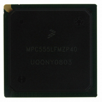
MPC555LFMZP40 Freescale Semiconductor, MPC555LFMZP40 Datasheet - Page 373

MPC555LFMZP40
Manufacturer Part Number
MPC555LFMZP40
Description
IC MCU 32BIT 40MHZ 272-BGA
Manufacturer
Freescale Semiconductor
Series
MPC5xxr
Datasheets
1.MPC555LFMZP40.pdf
(12 pages)
2.MPC555LFMZP40.pdf
(966 pages)
3.MPC555LFMZP40.pdf
(3 pages)
Specifications of MPC555LFMZP40
Core Processor
PowerPC
Core Size
32-Bit
Speed
40MHz
Connectivity
CAN, EBI/EMI, SCI, SPI, UART/USART
Peripherals
POR, PWM, WDT
Number Of I /o
101
Program Memory Size
448KB (448K x 8)
Program Memory Type
FLASH
Ram Size
26K x 8
Voltage - Supply (vcc/vdd)
2.5 V ~ 2.7 V
Data Converters
A/D 32x10b
Oscillator Type
External
Operating Temperature
-40°C ~ 125°C
Package / Case
272-PBGA
Controller Family/series
POWER 5xx
Ram Memory Size
26KB
Cpu Speed
63MIPS
Embedded Interface Type
QSPI, SCI, TouCAN
Operating Temperature Range
-40°C To +125°C
No. Of Pins
272
Rohs Compliant
No
Processor Series
MPC5xx
Core
PowerPC
Data Bus Width
32 bit
Data Ram Size
26 KB
Interface Type
CAN, QSPI, SCI
Maximum Clock Frequency
40 MHz
Number Of Programmable I/os
101
Operating Supply Voltage
3.3 V to 5 V
Maximum Operating Temperature
+ 125 C
Mounting Style
SMD/SMT
Development Tools By Supplier
MPC555CMEE
Minimum Operating Temperature
- 85 C
On-chip Adc
10 bit, 32 Channel
Cpu Family
MPC55xx
Device Core
PowerPC
Device Core Size
32b
Frequency (max)
40MHz
Total Internal Ram Size
32KB
# I/os (max)
101
Operating Supply Voltage (typ)
5V
Instruction Set Architecture
RISC
Operating Temp Range
-40C to 85C
Operating Temperature Classification
Industrial
Mounting
Surface Mount
Pin Count
272
Package Type
BGA
For Use With
MPC555CMEE - KIT EVAL FOR MPC555
Lead Free Status / RoHS Status
Contains lead / RoHS non-compliant
Eeprom Size
-
Lead Free Status / Rohs Status
No
Available stocks
Company
Part Number
Manufacturer
Quantity
Price
Company:
Part Number:
MPC555LFMZP40
Manufacturer:
MOTOLOLA
Quantity:
853
Company:
Part Number:
MPC555LFMZP40
Manufacturer:
Freescale Semiconductor
Quantity:
10 000
Company:
Part Number:
MPC555LFMZP40R2
Manufacturer:
Freescale Semiconductor
Quantity:
10 000
- Current page: 373 of 966
- Download datasheet (15Mb)
10.5 Write and Byte Enable Signals
10.6 Dual Mapping of the Internal Flash EEPROM Array
MPC555
USER’S MANUAL
Transfer
Word
Word
Size
Byte
Half-
The GPCM determines the timing and value of the WE/BE signals if allowed by the
port size of the accessed bank, the transfer size of the transaction and the address
accessed.
The functionality of the WE/BE[0:3] pins depends upon the value of the write enable/
byte select (WEBS) bit in the corresponding BR register. Setting WEBS to 1 will enable
these pins as BE, while resetting it to zero will enable them as WE. WE is asserted
only during write access, while BE is asserted for both read and write accesses. The
timing of the WE/BE pins remains the same in either case, and is determined by the
TRLX, ACS and CSNT bits.
The upper WE/BE (WE[0]/BE[0]) indicates that the upper eight bits of the data bus
(D0–D7) contains valid data during a write/read cycle. The upper-middle write byte en-
able (WE[1]/BE[1]) indicates that the upper-middle eight bits of the data bus (D8–D15)
contains valid data during a write/read cycle. The lower-middle write byte enable
(WE[2]/BE[2]) indicates that the lower-middle eight bits of the data bus (D16–D23)
contains valid data during a write/read cycle. The lower write/read enable (WE[3]/
BE[3]) indicates that the lower eight bits of the data bus contains valid data during a
write cycle.
The write/byte enable lines affected in a transaction for 32-bit port (PS = 00), a
16-bit port (PS = 10) and a 8-bit port (PS = 01) are shown in
shows which write enables are asserted (indicated with an ‘X’) for different combina-
tions of port size and transfer size
The user can enable mapping of the internal flash EEPROM (CMF) module to an ex-
ternal memory region controlled by the memory controller. Only one region can be pro-
grammed to be dual-mapped. When dual mapping is enabled (DME bit is set in
DMBR), an internal address matches the dual-mapped address range (as pro-
grammed in the DMBR), and the cycle type matches AT/ATM field in DMBR/DMOR
registers, then the following occur:
• The internal flash memory does not respond to that address
/
MPC556
TSIZ
0 1
0 1
0 1
0 1
1 0
1 0
0 0
A30 A31
Address
Table 10-4 Write Enable/Byte Enable Signals Function
0
0
1
1
0
1
0
0
1
0
1
0
0
0
Freescale Semiconductor, Inc.
WE[0]
BE[0]
For More Information On This Product,
X
X
X
/
32-bit Port Size
WE[1]
BE[1]
X
X
X
/
Go to: www.freescale.com
MEMORY CONTROLLER
Rev. 15 October 2000
WE[2]
BE[2]
X
X
X
/
WE[3]
BE[3]
X
X
X
/
WE[0]
BE[0]
X
X
X
X
X
/
16-bit Port Size
WE[1]
BE[1]
X
X
X
X
X
/
WE[2]
BE[2]
/
WE[3]
BE[3]
/
Table
WE[0]
BE[0]
X
X
X
X
X
X
X
/
8-bit Port Size
10-4. This table
WE[1]
BE[1]
/
MOTOROLA
WE[2]
BE[2]
/
10-21
WE[3]
BE[3]
/
Related parts for MPC555LFMZP40
Image
Part Number
Description
Manufacturer
Datasheet
Request
R
Part Number:
Description:
Manufacturer:
Freescale Semiconductor, Inc
Datasheet:
Part Number:
Description:
Manufacturer:
Freescale Semiconductor, Inc
Datasheet:
Part Number:
Description:
Manufacturer:
Freescale Semiconductor, Inc
Datasheet:
Part Number:
Description:
Manufacturer:
Freescale Semiconductor, Inc
Datasheet:
Part Number:
Description:
Manufacturer:
Freescale Semiconductor, Inc
Datasheet:
Part Number:
Description:
Manufacturer:
Freescale Semiconductor, Inc
Datasheet:
Part Number:
Description:
Manufacturer:
Freescale Semiconductor, Inc
Datasheet:
Part Number:
Description:
Manufacturer:
Freescale Semiconductor, Inc
Datasheet:
Part Number:
Description:
Manufacturer:
Freescale Semiconductor, Inc
Datasheet:
Part Number:
Description:
Manufacturer:
Freescale Semiconductor, Inc
Datasheet:
Part Number:
Description:
Manufacturer:
Freescale Semiconductor, Inc
Datasheet:
Part Number:
Description:
Manufacturer:
Freescale Semiconductor, Inc
Datasheet:
Part Number:
Description:
Manufacturer:
Freescale Semiconductor, Inc
Datasheet:
Part Number:
Description:
Manufacturer:
Freescale Semiconductor, Inc
Datasheet:
Part Number:
Description:
Manufacturer:
Freescale Semiconductor, Inc
Datasheet:


