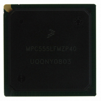
MPC555LFMZP40 Freescale Semiconductor, MPC555LFMZP40 Datasheet - Page 727

MPC555LFMZP40
Manufacturer Part Number
MPC555LFMZP40
Description
IC MCU 32BIT 40MHZ 272-BGA
Manufacturer
Freescale Semiconductor
Series
MPC5xxr
Datasheets
1.MPC555LFMZP40.pdf
(12 pages)
2.MPC555LFMZP40.pdf
(966 pages)
3.MPC555LFMZP40.pdf
(3 pages)
Specifications of MPC555LFMZP40
Core Processor
PowerPC
Core Size
32-Bit
Speed
40MHz
Connectivity
CAN, EBI/EMI, SCI, SPI, UART/USART
Peripherals
POR, PWM, WDT
Number Of I /o
101
Program Memory Size
448KB (448K x 8)
Program Memory Type
FLASH
Ram Size
26K x 8
Voltage - Supply (vcc/vdd)
2.5 V ~ 2.7 V
Data Converters
A/D 32x10b
Oscillator Type
External
Operating Temperature
-40°C ~ 125°C
Package / Case
272-PBGA
Controller Family/series
POWER 5xx
Ram Memory Size
26KB
Cpu Speed
63MIPS
Embedded Interface Type
QSPI, SCI, TouCAN
Operating Temperature Range
-40°C To +125°C
No. Of Pins
272
Rohs Compliant
No
Processor Series
MPC5xx
Core
PowerPC
Data Bus Width
32 bit
Data Ram Size
26 KB
Interface Type
CAN, QSPI, SCI
Maximum Clock Frequency
40 MHz
Number Of Programmable I/os
101
Operating Supply Voltage
3.3 V to 5 V
Maximum Operating Temperature
+ 125 C
Mounting Style
SMD/SMT
Development Tools By Supplier
MPC555CMEE
Minimum Operating Temperature
- 85 C
On-chip Adc
10 bit, 32 Channel
Cpu Family
MPC55xx
Device Core
PowerPC
Device Core Size
32b
Frequency (max)
40MHz
Total Internal Ram Size
32KB
# I/os (max)
101
Operating Supply Voltage (typ)
5V
Instruction Set Architecture
RISC
Operating Temp Range
-40C to 85C
Operating Temperature Classification
Industrial
Mounting
Surface Mount
Pin Count
272
Package Type
BGA
For Use With
MPC555CMEE - KIT EVAL FOR MPC555
Lead Free Status / RoHS Status
Contains lead / RoHS non-compliant
Eeprom Size
-
Lead Free Status / Rohs Status
No
Available stocks
Company
Part Number
Manufacturer
Quantity
Price
Company:
Part Number:
MPC555LFMZP40
Manufacturer:
MOTOLOLA
Quantity:
853
Company:
Part Number:
MPC555LFMZP40
Manufacturer:
Freescale Semiconductor
Quantity:
10 000
Company:
Part Number:
MPC555LFMZP40R2
Manufacturer:
Freescale Semiconductor
Quantity:
10 000
- Current page: 727 of 966
- Download datasheet (15Mb)
21.5 Development Port
21.5.1 Development Port Pins
21.5.2 Development Serial Clock
21.5.3 Development Serial Data In
MPC555
USER’S MANUAL
performing the rfi. Failing to do so will force the CPU to immediately re-enter to debug
mode and to re-assert the freeze indication in case an asserted bit in the interrupt
cause register (ECR) has a corresponding enable bit set in the debug enable register
(DER).
The development port provides a full duplex serial interface for communications be-
tween the internal development support logic including debug mode and an external
development tool.
The relationship of the development support logic to the rest of the CPU chip is shown
in
clarity. It is implemented as part of the SIU module.
The following development port pin functions are provided:
The development serial clock (DSCK) is used to shift data into and out of the develop-
ment port shift register. At the same time, the new most significant bit of the shift reg-
ister is presented at the DSDO pin. In all further discussions references to the DSCK
signal imply the internal synchronized value of the clock. The DSCK input must be driv-
en either high or low at all times and not allowed to float. A typical target environment
would pull this input low with a resistor.
The clock may be implemented as a free running clock or as gated clock. As discussed
in section
Mode
Mode, the shifting of data is controlled by ready and start signals so the clock does not
need to be gated with the serial transmissions.
The DSCK pin is also used at reset to enable debug mode and immediately following
reset to optionally cause immediate entry into debug mode following reset.
Data to be transferred into the development port shift register is presented at the de-
velopment serial data in (DSDI) pin by external logic. To be sure that the correct value
is used internally. When driven asynchronous (synchronous) with the system clock,
the data presented to DSDI must be stable a setup time before the rising edge of
DSCK (CLKOUT) and a hold time after the rising edge of DSCK (CLKOUT).
Figure
1. Development serial clock (DSCK)
2. Development serial data in (DSDI)
3. Development serial data out (DSDO)
/
MPC556
and section
21-5. The development port support logic is shown as a separate block for
21.5.6.5 Development Port Serial Communications — Trap Enable
21.5.6.8 Development Port Serial Communications — Debug
Freescale Semiconductor, Inc.
For More Information On This Product,
DEVELOPMENT SUPPORT
Go to: www.freescale.com
Rev. 15 October 2000
MOTOROLA
21-31
Related parts for MPC555LFMZP40
Image
Part Number
Description
Manufacturer
Datasheet
Request
R
Part Number:
Description:
Manufacturer:
Freescale Semiconductor, Inc
Datasheet:
Part Number:
Description:
Manufacturer:
Freescale Semiconductor, Inc
Datasheet:
Part Number:
Description:
Manufacturer:
Freescale Semiconductor, Inc
Datasheet:
Part Number:
Description:
Manufacturer:
Freescale Semiconductor, Inc
Datasheet:
Part Number:
Description:
Manufacturer:
Freescale Semiconductor, Inc
Datasheet:
Part Number:
Description:
Manufacturer:
Freescale Semiconductor, Inc
Datasheet:
Part Number:
Description:
Manufacturer:
Freescale Semiconductor, Inc
Datasheet:
Part Number:
Description:
Manufacturer:
Freescale Semiconductor, Inc
Datasheet:
Part Number:
Description:
Manufacturer:
Freescale Semiconductor, Inc
Datasheet:
Part Number:
Description:
Manufacturer:
Freescale Semiconductor, Inc
Datasheet:
Part Number:
Description:
Manufacturer:
Freescale Semiconductor, Inc
Datasheet:
Part Number:
Description:
Manufacturer:
Freescale Semiconductor, Inc
Datasheet:
Part Number:
Description:
Manufacturer:
Freescale Semiconductor, Inc
Datasheet:
Part Number:
Description:
Manufacturer:
Freescale Semiconductor, Inc
Datasheet:
Part Number:
Description:
Manufacturer:
Freescale Semiconductor, Inc
Datasheet:


