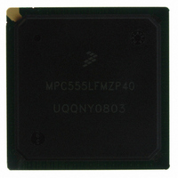
MPC555LFMZP40 Freescale Semiconductor, MPC555LFMZP40 Datasheet - Page 539

MPC555LFMZP40
Manufacturer Part Number
MPC555LFMZP40
Description
IC MCU 32BIT 40MHZ 272-BGA
Manufacturer
Freescale Semiconductor
Series
MPC5xxr
Datasheets
1.MPC555LFMZP40.pdf
(12 pages)
2.MPC555LFMZP40.pdf
(966 pages)
3.MPC555LFMZP40.pdf
(3 pages)
Specifications of MPC555LFMZP40
Core Processor
PowerPC
Core Size
32-Bit
Speed
40MHz
Connectivity
CAN, EBI/EMI, SCI, SPI, UART/USART
Peripherals
POR, PWM, WDT
Number Of I /o
101
Program Memory Size
448KB (448K x 8)
Program Memory Type
FLASH
Ram Size
26K x 8
Voltage - Supply (vcc/vdd)
2.5 V ~ 2.7 V
Data Converters
A/D 32x10b
Oscillator Type
External
Operating Temperature
-40°C ~ 125°C
Package / Case
272-PBGA
Controller Family/series
POWER 5xx
Ram Memory Size
26KB
Cpu Speed
63MIPS
Embedded Interface Type
QSPI, SCI, TouCAN
Operating Temperature Range
-40°C To +125°C
No. Of Pins
272
Rohs Compliant
No
Processor Series
MPC5xx
Core
PowerPC
Data Bus Width
32 bit
Data Ram Size
26 KB
Interface Type
CAN, QSPI, SCI
Maximum Clock Frequency
40 MHz
Number Of Programmable I/os
101
Operating Supply Voltage
3.3 V to 5 V
Maximum Operating Temperature
+ 125 C
Mounting Style
SMD/SMT
Development Tools By Supplier
MPC555CMEE
Minimum Operating Temperature
- 85 C
On-chip Adc
10 bit, 32 Channel
Cpu Family
MPC55xx
Device Core
PowerPC
Device Core Size
32b
Frequency (max)
40MHz
Total Internal Ram Size
32KB
# I/os (max)
101
Operating Supply Voltage (typ)
5V
Instruction Set Architecture
RISC
Operating Temp Range
-40C to 85C
Operating Temperature Classification
Industrial
Mounting
Surface Mount
Pin Count
272
Package Type
BGA
For Use With
MPC555CMEE - KIT EVAL FOR MPC555
Lead Free Status / RoHS Status
Contains lead / RoHS non-compliant
Eeprom Size
-
Lead Free Status / Rohs Status
No
Available stocks
Company
Part Number
Manufacturer
Quantity
Price
Company:
Part Number:
MPC555LFMZP40
Manufacturer:
MOTOLOLA
Quantity:
853
Company:
Part Number:
MPC555LFMZP40
Manufacturer:
Freescale Semiconductor
Quantity:
10 000
Company:
Part Number:
MPC555LFMZP40R2
Manufacturer:
Freescale Semiconductor
Quantity:
10 000
- Current page: 539 of 966
- Download datasheet (15Mb)
15.2 Submodule Numbering, Naming and Addressing
15.3 MIOS1 Signals
MPC555
USER’S MANUAL
A block is a group of four 16-bit registers. Each of the blocks within the MIOS1 ad-
dressing range is assigned a block number. The first block is located at the base ad-
dress of the MIOS1. The blocks are numbered sequentially starting from 0.
Every submodule instantiation is also assigned a number. The number of a given sub-
module is the block number of the first block of this submodule.
A submodule is assigned a name made of its acronym followed by its submodule num-
ber. For example, if submodule number 18 were an MPWMSM, it would be named
MPWMSM18.
This numbering convention does not apply to the MBISM, the MCPSM and the
MIRSMs. The MBISM and the MCPSM are unique in the MIOS1 and do not need a
number. The MIRSMs are numbered incrementally starting from zero.
The MIOS1 base address is defined at the chip level and is referred to as the “MIOS1
base address.” The MIOS1 addressable range is four Kbytes.
The base address of a given implemented submodule within the MIOS1 is the sum of
the base address of the MIOS1 and the submodule number multiplied by eight. (Refer
to
This does not apply to the MBISM, the MCPSM and the MIRSMs. For these submod-
ules, refer to the MIOS1 memory map
The MIOS1 requires 34 pins: 10 MDASM pins, eight MPWMSM pins and 16 MPIOSM
pins. The usage of these pins is shown in the block diagram of
configuration description of
MDA, MPWMSM pins have a prefix of MPWM and the port pins have a prefix of MPIO.
The modulus counter clock and load pins are multiplexed with MDASM pins.
The MIOS1 input and output pin names are composed of five fields according to the
following convention:
Table
• MIOS 16-bit parallel port I/O submodule (MPIOSM):
• “M”
• <submodule short_prefix>
• <submodule number>
• <pin attribute suffix> (optional)
• <bit number> (optional)
/
— Software selectable output pulse polarity
— Software readable output pin status
— Possible use of pin as I/O port when PWM function is not needed
— 16 parallel input/output pins
— Simple data direction register (DDR) concept for selection of pin direction
MPC556
15-36.)
MODULAR INPUT/OUTPUT SUBSYSTEM (MIOS1)
Freescale Semiconductor, Inc.
For More Information On This Product,
Table
Go to: www.freescale.com
Rev. 15 October 2000
15-36. In the figure, MDASM pins have a prefix
(Figure
15-2).
Figure 15-1
MOTOROLA
and in the
15-3
Related parts for MPC555LFMZP40
Image
Part Number
Description
Manufacturer
Datasheet
Request
R
Part Number:
Description:
Manufacturer:
Freescale Semiconductor, Inc
Datasheet:
Part Number:
Description:
Manufacturer:
Freescale Semiconductor, Inc
Datasheet:
Part Number:
Description:
Manufacturer:
Freescale Semiconductor, Inc
Datasheet:
Part Number:
Description:
Manufacturer:
Freescale Semiconductor, Inc
Datasheet:
Part Number:
Description:
Manufacturer:
Freescale Semiconductor, Inc
Datasheet:
Part Number:
Description:
Manufacturer:
Freescale Semiconductor, Inc
Datasheet:
Part Number:
Description:
Manufacturer:
Freescale Semiconductor, Inc
Datasheet:
Part Number:
Description:
Manufacturer:
Freescale Semiconductor, Inc
Datasheet:
Part Number:
Description:
Manufacturer:
Freescale Semiconductor, Inc
Datasheet:
Part Number:
Description:
Manufacturer:
Freescale Semiconductor, Inc
Datasheet:
Part Number:
Description:
Manufacturer:
Freescale Semiconductor, Inc
Datasheet:
Part Number:
Description:
Manufacturer:
Freescale Semiconductor, Inc
Datasheet:
Part Number:
Description:
Manufacturer:
Freescale Semiconductor, Inc
Datasheet:
Part Number:
Description:
Manufacturer:
Freescale Semiconductor, Inc
Datasheet:
Part Number:
Description:
Manufacturer:
Freescale Semiconductor, Inc
Datasheet:


