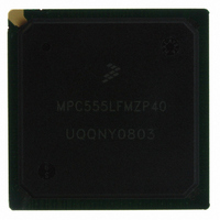
MPC555LFMZP40 Freescale Semiconductor, MPC555LFMZP40 Datasheet - Page 426

MPC555LFMZP40
Manufacturer Part Number
MPC555LFMZP40
Description
IC MCU 32BIT 40MHZ 272-BGA
Manufacturer
Freescale Semiconductor
Series
MPC5xxr
Datasheets
1.MPC555LFMZP40.pdf
(12 pages)
2.MPC555LFMZP40.pdf
(966 pages)
3.MPC555LFMZP40.pdf
(3 pages)
Specifications of MPC555LFMZP40
Core Processor
PowerPC
Core Size
32-Bit
Speed
40MHz
Connectivity
CAN, EBI/EMI, SCI, SPI, UART/USART
Peripherals
POR, PWM, WDT
Number Of I /o
101
Program Memory Size
448KB (448K x 8)
Program Memory Type
FLASH
Ram Size
26K x 8
Voltage - Supply (vcc/vdd)
2.5 V ~ 2.7 V
Data Converters
A/D 32x10b
Oscillator Type
External
Operating Temperature
-40°C ~ 125°C
Package / Case
272-PBGA
Controller Family/series
POWER 5xx
Ram Memory Size
26KB
Cpu Speed
63MIPS
Embedded Interface Type
QSPI, SCI, TouCAN
Operating Temperature Range
-40°C To +125°C
No. Of Pins
272
Rohs Compliant
No
Processor Series
MPC5xx
Core
PowerPC
Data Bus Width
32 bit
Data Ram Size
26 KB
Interface Type
CAN, QSPI, SCI
Maximum Clock Frequency
40 MHz
Number Of Programmable I/os
101
Operating Supply Voltage
3.3 V to 5 V
Maximum Operating Temperature
+ 125 C
Mounting Style
SMD/SMT
Development Tools By Supplier
MPC555CMEE
Minimum Operating Temperature
- 85 C
On-chip Adc
10 bit, 32 Channel
Cpu Family
MPC55xx
Device Core
PowerPC
Device Core Size
32b
Frequency (max)
40MHz
Total Internal Ram Size
32KB
# I/os (max)
101
Operating Supply Voltage (typ)
5V
Instruction Set Architecture
RISC
Operating Temp Range
-40C to 85C
Operating Temperature Classification
Industrial
Mounting
Surface Mount
Pin Count
272
Package Type
BGA
For Use With
MPC555CMEE - KIT EVAL FOR MPC555
Lead Free Status / RoHS Status
Contains lead / RoHS non-compliant
Eeprom Size
-
Lead Free Status / Rohs Status
No
Available stocks
Company
Part Number
Manufacturer
Quantity
Price
Company:
Part Number:
MPC555LFMZP40
Manufacturer:
MOTOLOLA
Quantity:
853
Company:
Part Number:
MPC555LFMZP40
Manufacturer:
Freescale Semiconductor
Quantity:
10 000
Company:
Part Number:
MPC555LFMZP40R2
Manufacturer:
Freescale Semiconductor
Quantity:
10 000
- Current page: 426 of 966
- Download datasheet (15Mb)
13.9.2 Front-End Analog Multiplexer
13.9.3 Digital-to-Analog Converter Array
13.9.4 Comparator
13.9.5 Successive Approximation Register
13.10 Digital Control Subsystem
MPC555
USER’S MANUAL
The internal multiplexer selects one of the 16 analog input pins or one of three special
internal reference channels for conversion. The following are the three special chan-
nels:
The selected input is connected to one side of the DAC capacitor array. The other side
of the DAC array is connected to the comparator input. The multiplexer also includes
positive and negative stress protection circuitry, which prevents other channels from
affecting the present conversion when excessive voltage levels are applied to the oth-
er channels.
The digital-to-analog converter (DAC) array consists of binary-weighted capacitors
and a resistor-divider chain. The array serves two purposes:
Resolution begins with the MSB and works down to the LSB. The switching sequence
is controlled by the SAR logic.
The comparator is used during the approximation process to sense whether the digi-
tally selected arrangement of the DAC array produces a voltage level higher or lower
than the sampled input. The comparator output feeds into the SAR which accumulates
the A/D conversion result sequentially, starting with the MSB.
The input of the successive approximation register (SAR) is connected to the compar-
ator output. The SAR sequentially receives the conversion value one bit at a time,
starting with the MSB. After accumulating the ten bits of the conversion result, the SAR
data is transferred by the queue control logic in the digital section to the appropriate
result location, where it may be read by user software.
The digital control subsystem includes the clock and periodic/interval timer, control
and status registers, the conversion command word table RAM, and the result word
table RAM.
The central element for control of the QADC64 conversions is the 64-entry CCW table.
Each CCW specifies the conversion of one input channel. Depending on the applica-
tion, one or two queues can be established in the CCW table. A queue is a scan se-
quence of one or more input channels. By using a pause mechanism, sub-queues can
• V
• V
• (V
• The array holds the sampled input voltage during conversion
• The resistor-capacitor array provides the mechanism for the successive approx-
/
imation A/D conversion
MPC556 QUEUED ANALOG-TO-DIGITAL CONVERTER MODULE-64
RH
RL
RH
— Reference Voltage Low
— Reference Voltage High
– V
RL
)/2 — Mid-Reference Voltage
Freescale Semiconductor, Inc.
For More Information On This Product,
Go to: www.freescale.com
Rev. 15 October 2000
MOTOROLA
13-14
Related parts for MPC555LFMZP40
Image
Part Number
Description
Manufacturer
Datasheet
Request
R
Part Number:
Description:
Manufacturer:
Freescale Semiconductor, Inc
Datasheet:
Part Number:
Description:
Manufacturer:
Freescale Semiconductor, Inc
Datasheet:
Part Number:
Description:
Manufacturer:
Freescale Semiconductor, Inc
Datasheet:
Part Number:
Description:
Manufacturer:
Freescale Semiconductor, Inc
Datasheet:
Part Number:
Description:
Manufacturer:
Freescale Semiconductor, Inc
Datasheet:
Part Number:
Description:
Manufacturer:
Freescale Semiconductor, Inc
Datasheet:
Part Number:
Description:
Manufacturer:
Freescale Semiconductor, Inc
Datasheet:
Part Number:
Description:
Manufacturer:
Freescale Semiconductor, Inc
Datasheet:
Part Number:
Description:
Manufacturer:
Freescale Semiconductor, Inc
Datasheet:
Part Number:
Description:
Manufacturer:
Freescale Semiconductor, Inc
Datasheet:
Part Number:
Description:
Manufacturer:
Freescale Semiconductor, Inc
Datasheet:
Part Number:
Description:
Manufacturer:
Freescale Semiconductor, Inc
Datasheet:
Part Number:
Description:
Manufacturer:
Freescale Semiconductor, Inc
Datasheet:
Part Number:
Description:
Manufacturer:
Freescale Semiconductor, Inc
Datasheet:
Part Number:
Description:
Manufacturer:
Freescale Semiconductor, Inc
Datasheet:


