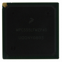
MPC555LFMZP40 Freescale Semiconductor, MPC555LFMZP40 Datasheet - Page 698

MPC555LFMZP40
Manufacturer Part Number
MPC555LFMZP40
Description
IC MCU 32BIT 40MHZ 272-BGA
Manufacturer
Freescale Semiconductor
Series
MPC5xxr
Datasheets
1.MPC555LFMZP40.pdf
(12 pages)
2.MPC555LFMZP40.pdf
(966 pages)
3.MPC555LFMZP40.pdf
(3 pages)
Specifications of MPC555LFMZP40
Core Processor
PowerPC
Core Size
32-Bit
Speed
40MHz
Connectivity
CAN, EBI/EMI, SCI, SPI, UART/USART
Peripherals
POR, PWM, WDT
Number Of I /o
101
Program Memory Size
448KB (448K x 8)
Program Memory Type
FLASH
Ram Size
26K x 8
Voltage - Supply (vcc/vdd)
2.5 V ~ 2.7 V
Data Converters
A/D 32x10b
Oscillator Type
External
Operating Temperature
-40°C ~ 125°C
Package / Case
272-PBGA
Controller Family/series
POWER 5xx
Ram Memory Size
26KB
Cpu Speed
63MIPS
Embedded Interface Type
QSPI, SCI, TouCAN
Operating Temperature Range
-40°C To +125°C
No. Of Pins
272
Rohs Compliant
No
Processor Series
MPC5xx
Core
PowerPC
Data Bus Width
32 bit
Data Ram Size
26 KB
Interface Type
CAN, QSPI, SCI
Maximum Clock Frequency
40 MHz
Number Of Programmable I/os
101
Operating Supply Voltage
3.3 V to 5 V
Maximum Operating Temperature
+ 125 C
Mounting Style
SMD/SMT
Development Tools By Supplier
MPC555CMEE
Minimum Operating Temperature
- 85 C
On-chip Adc
10 bit, 32 Channel
Cpu Family
MPC55xx
Device Core
PowerPC
Device Core Size
32b
Frequency (max)
40MHz
Total Internal Ram Size
32KB
# I/os (max)
101
Operating Supply Voltage (typ)
5V
Instruction Set Architecture
RISC
Operating Temp Range
-40C to 85C
Operating Temperature Classification
Industrial
Mounting
Surface Mount
Pin Count
272
Package Type
BGA
For Use With
MPC555CMEE - KIT EVAL FOR MPC555
Lead Free Status / RoHS Status
Contains lead / RoHS non-compliant
Eeprom Size
-
Lead Free Status / Rohs Status
No
Available stocks
Company
Part Number
Manufacturer
Quantity
Price
Company:
Part Number:
MPC555LFMZP40
Manufacturer:
MOTOLOLA
Quantity:
853
Company:
Part Number:
MPC555LFMZP40
Manufacturer:
Freescale Semiconductor
Quantity:
10 000
Company:
Part Number:
MPC555LFMZP40R2
Manufacturer:
Freescale Semiconductor
Quantity:
10 000
- Current page: 698 of 966
- Download datasheet (15Mb)
21.2.1 Program Trace Cycle
MPC555
USER’S MANUAL
Instructions are fetched sequentially until branches (direct or indirect) or exceptions
appear in the program flow or some stall in execution causes the machine not to fetch
the next address. Instructions may be architecturally executed, or they may be can-
celed in some stage of the machine pipeline.
The following sections define how this information is generated and how it should be
used to reconstruct the program trace. The issue of data compression that could re-
duce the amount of memory needed by the debug system is also mentioned.
To allow visibility of the events happening in the machine a few dedicated pins are
used and a special bus cycle attribute, program trace cycle, is defined.
The program trace cycle attribute is attached to all fetch cycles resulting from indirect
flow changes. When program trace recording is needed, the user can make sure these
cycles are visible on the external bus.
The VSYNC indication, when asserted, forces all fetch cycles marked with the pro-
gram trace cycle attribute to be visible on the external bus even if their data is found
in one of the internal devices. To enable the external hardware to properly synchronize
with the internal activity of the CPU, the assertion and negation of VSYNC forces the
machine to synchronize. The first fetch after this synchronization is marked as a pro-
gram trace cycle and is visible on the external bus. For more information on the activity
of the external hardware during program trace refer to
In order to keep the pin count of the chip as low as possible, VSYNC is not implement-
ed as one of the chip’s external pins. It is asserted and negated using the serial inter-
face implemented in the development port. For more information on this interface refer
to
Forcing the CPU to show all fetch cycles marked with the program trace cycle attribute
can be done either by asserting the VSYNC pin (as mentioned above) or by program-
ming the fetch show cycle bits in the instruction support control register, ICTRL. For
more information refer to
When the VSYNC indication is asserted, all fetch cycles marked with the program
trace cycle attribute are made visible on the external bus. These cycles can generate
regular bus cycles (address phase and data phase) when the instructions reside only
in one of the external devices. Or, they can generate address-only cycles when the
instructions reside in one of the internal devices (internal memory, etc.).
When VSYNC is asserted, some performance degradation is expected due to the ad-
ditional external bus cycles. However, since this performance degradation is expected
to be very small, it is possible to program the machine to show all indirect flow chang-
es. In this way, the machine will always perform the additional external bus cycles and
maintain exactly the same behavior both when VSYNC is asserted and when it is ne-
gated. For more information refer to
21.5 Development Port
• The number of instructions canceled each clock
/
MPC556
Freescale Semiconductor, Inc.
For More Information On This Product,
21.2.5 Instruction Fetch Show Cycle Control
DEVELOPMENT SUPPORT
Go to: www.freescale.com
Rev. 15 October 2000
21.7.6 I-Bus Support Control
21.2.4 The External
Register.
Hardware.
MOTOROLA
21-2
Related parts for MPC555LFMZP40
Image
Part Number
Description
Manufacturer
Datasheet
Request
R
Part Number:
Description:
Manufacturer:
Freescale Semiconductor, Inc
Datasheet:
Part Number:
Description:
Manufacturer:
Freescale Semiconductor, Inc
Datasheet:
Part Number:
Description:
Manufacturer:
Freescale Semiconductor, Inc
Datasheet:
Part Number:
Description:
Manufacturer:
Freescale Semiconductor, Inc
Datasheet:
Part Number:
Description:
Manufacturer:
Freescale Semiconductor, Inc
Datasheet:
Part Number:
Description:
Manufacturer:
Freescale Semiconductor, Inc
Datasheet:
Part Number:
Description:
Manufacturer:
Freescale Semiconductor, Inc
Datasheet:
Part Number:
Description:
Manufacturer:
Freescale Semiconductor, Inc
Datasheet:
Part Number:
Description:
Manufacturer:
Freescale Semiconductor, Inc
Datasheet:
Part Number:
Description:
Manufacturer:
Freescale Semiconductor, Inc
Datasheet:
Part Number:
Description:
Manufacturer:
Freescale Semiconductor, Inc
Datasheet:
Part Number:
Description:
Manufacturer:
Freescale Semiconductor, Inc
Datasheet:
Part Number:
Description:
Manufacturer:
Freescale Semiconductor, Inc
Datasheet:
Part Number:
Description:
Manufacturer:
Freescale Semiconductor, Inc
Datasheet:
Part Number:
Description:
Manufacturer:
Freescale Semiconductor, Inc
Datasheet:


