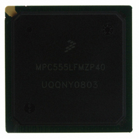
MPC555LFMZP40 Freescale Semiconductor, MPC555LFMZP40 Datasheet - Page 675

MPC555LFMZP40
Manufacturer Part Number
MPC555LFMZP40
Description
IC MCU 32BIT 40MHZ 272-BGA
Manufacturer
Freescale Semiconductor
Series
MPC5xxr
Datasheets
1.MPC555LFMZP40.pdf
(12 pages)
2.MPC555LFMZP40.pdf
(966 pages)
3.MPC555LFMZP40.pdf
(3 pages)
Specifications of MPC555LFMZP40
Core Processor
PowerPC
Core Size
32-Bit
Speed
40MHz
Connectivity
CAN, EBI/EMI, SCI, SPI, UART/USART
Peripherals
POR, PWM, WDT
Number Of I /o
101
Program Memory Size
448KB (448K x 8)
Program Memory Type
FLASH
Ram Size
26K x 8
Voltage - Supply (vcc/vdd)
2.5 V ~ 2.7 V
Data Converters
A/D 32x10b
Oscillator Type
External
Operating Temperature
-40°C ~ 125°C
Package / Case
272-PBGA
Controller Family/series
POWER 5xx
Ram Memory Size
26KB
Cpu Speed
63MIPS
Embedded Interface Type
QSPI, SCI, TouCAN
Operating Temperature Range
-40°C To +125°C
No. Of Pins
272
Rohs Compliant
No
Processor Series
MPC5xx
Core
PowerPC
Data Bus Width
32 bit
Data Ram Size
26 KB
Interface Type
CAN, QSPI, SCI
Maximum Clock Frequency
40 MHz
Number Of Programmable I/os
101
Operating Supply Voltage
3.3 V to 5 V
Maximum Operating Temperature
+ 125 C
Mounting Style
SMD/SMT
Development Tools By Supplier
MPC555CMEE
Minimum Operating Temperature
- 85 C
On-chip Adc
10 bit, 32 Channel
Cpu Family
MPC55xx
Device Core
PowerPC
Device Core Size
32b
Frequency (max)
40MHz
Total Internal Ram Size
32KB
# I/os (max)
101
Operating Supply Voltage (typ)
5V
Instruction Set Architecture
RISC
Operating Temp Range
-40C to 85C
Operating Temperature Classification
Industrial
Mounting
Surface Mount
Pin Count
272
Package Type
BGA
For Use With
MPC555CMEE - KIT EVAL FOR MPC555
Lead Free Status / RoHS Status
Contains lead / RoHS non-compliant
Eeprom Size
-
Lead Free Status / Rohs Status
No
Available stocks
Company
Part Number
Manufacturer
Quantity
Price
Company:
Part Number:
MPC555LFMZP40
Manufacturer:
MOTOLOLA
Quantity:
853
Company:
Part Number:
MPC555LFMZP40
Manufacturer:
Freescale Semiconductor
Quantity:
10 000
Company:
Part Number:
MPC555LFMZP40R2
Manufacturer:
Freescale Semiconductor
Quantity:
10 000
- Current page: 675 of 966
- Download datasheet (15Mb)
19.5.3 Over-Programming
19.6 Erasing CMF Array Blocks
19.6.1 Erase Sequence
MPC555
USER’S MANUAL
Either of the following events results in an over-programmed state:
Once a CMF bit has been over-programmed, data in the array block (32 Kbytes) that
is located in the same column is lost, since the over-programmed bit causes the entire
column to appear programmed. To restore an array block with an over-programmed
bit, the block must be erased.
To modify the charge stored in the isolated element of the CMF bit from a logic zero
state to a logic one state, an erase operation is required. The erase operation cannot
change the logic one state to a logic zero state; this is accomplished by the program
operation. In the CMF EEPROM, erase is a bulk operation that affects the stored
charge of all the isolated elements in an array block.
To make the CMF module block-erasable, the array is divided into blocks that are
physically isolated from each other. Each of the array blocks may be erased in isola-
tion or in any combination. The CMF array block size is fixed for all blocks in the mod-
ule at 32 Kbytes. CMF module A consists of eight array blocks; CMF module B
consists of six blocks. Array blocks of the CMF EEPROM that are protected (PRO-
TECT[M] = 1) are not erased. In addition, if EPEE = 0 no erase voltages are applied
to the array.
The array blocks selected for erase operation are determined by BLOCK[0:7] and the
array configuration.
The CMF EEPROM module requires a sequence of writes to the high voltage control
register (CMFCTL) and an erase interlock write in order to enable the high voltage to
the array and shadow information for erase operation. See
rithm bit settings.The erase sequence follows.
• Programming a CMF bit without a program margin read after each program pulse
• Exceeding the specified program times or voltages
1. Write PROTECT[0:7] to disable protect for the blocks to be erased.
2. Write PAWS to 0b100, NVR to 1, and GDB to 1.
3. Using
/
MPC556
the pulse width timing control fields for an erase pulse, BLOCK[0:7] to select the
blocks to be erased, PE = 1 and SES = 1 in the CMFCTL register. Set the initial
Failure to read each page that is being programmed after each pro-
gram pulse may result in the loss of information in the CMF EEPROM
array. While this will not physically damage the array a full erase of
all blocks being programmed must be performed before the CMF EE-
PROM can be used reliably. For more information, see
Programming.
19.7.6 A Technique to Determine SCLKR, CLKPE, and
Freescale Semiconductor, Inc.
For More Information On This Product,
CDR MoneT FLASH EEPROM
Go to: www.freescale.com
Rev. 15 October 2000
CAUTION
Table 19-5
19.5.3 Over-
for erase algo-
CLKPM, write
MOTOROLA
19-23
Related parts for MPC555LFMZP40
Image
Part Number
Description
Manufacturer
Datasheet
Request
R
Part Number:
Description:
Manufacturer:
Freescale Semiconductor, Inc
Datasheet:
Part Number:
Description:
Manufacturer:
Freescale Semiconductor, Inc
Datasheet:
Part Number:
Description:
Manufacturer:
Freescale Semiconductor, Inc
Datasheet:
Part Number:
Description:
Manufacturer:
Freescale Semiconductor, Inc
Datasheet:
Part Number:
Description:
Manufacturer:
Freescale Semiconductor, Inc
Datasheet:
Part Number:
Description:
Manufacturer:
Freescale Semiconductor, Inc
Datasheet:
Part Number:
Description:
Manufacturer:
Freescale Semiconductor, Inc
Datasheet:
Part Number:
Description:
Manufacturer:
Freescale Semiconductor, Inc
Datasheet:
Part Number:
Description:
Manufacturer:
Freescale Semiconductor, Inc
Datasheet:
Part Number:
Description:
Manufacturer:
Freescale Semiconductor, Inc
Datasheet:
Part Number:
Description:
Manufacturer:
Freescale Semiconductor, Inc
Datasheet:
Part Number:
Description:
Manufacturer:
Freescale Semiconductor, Inc
Datasheet:
Part Number:
Description:
Manufacturer:
Freescale Semiconductor, Inc
Datasheet:
Part Number:
Description:
Manufacturer:
Freescale Semiconductor, Inc
Datasheet:
Part Number:
Description:
Manufacturer:
Freescale Semiconductor, Inc
Datasheet:


