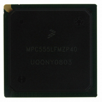
MPC555LFMZP40 Freescale Semiconductor, MPC555LFMZP40 Datasheet - Page 722

MPC555LFMZP40
Manufacturer Part Number
MPC555LFMZP40
Description
IC MCU 32BIT 40MHZ 272-BGA
Manufacturer
Freescale Semiconductor
Series
MPC5xxr
Datasheets
1.MPC555LFMZP40.pdf
(12 pages)
2.MPC555LFMZP40.pdf
(966 pages)
3.MPC555LFMZP40.pdf
(3 pages)
Specifications of MPC555LFMZP40
Core Processor
PowerPC
Core Size
32-Bit
Speed
40MHz
Connectivity
CAN, EBI/EMI, SCI, SPI, UART/USART
Peripherals
POR, PWM, WDT
Number Of I /o
101
Program Memory Size
448KB (448K x 8)
Program Memory Type
FLASH
Ram Size
26K x 8
Voltage - Supply (vcc/vdd)
2.5 V ~ 2.7 V
Data Converters
A/D 32x10b
Oscillator Type
External
Operating Temperature
-40°C ~ 125°C
Package / Case
272-PBGA
Controller Family/series
POWER 5xx
Ram Memory Size
26KB
Cpu Speed
63MIPS
Embedded Interface Type
QSPI, SCI, TouCAN
Operating Temperature Range
-40°C To +125°C
No. Of Pins
272
Rohs Compliant
No
Processor Series
MPC5xx
Core
PowerPC
Data Bus Width
32 bit
Data Ram Size
26 KB
Interface Type
CAN, QSPI, SCI
Maximum Clock Frequency
40 MHz
Number Of Programmable I/os
101
Operating Supply Voltage
3.3 V to 5 V
Maximum Operating Temperature
+ 125 C
Mounting Style
SMD/SMT
Development Tools By Supplier
MPC555CMEE
Minimum Operating Temperature
- 85 C
On-chip Adc
10 bit, 32 Channel
Cpu Family
MPC55xx
Device Core
PowerPC
Device Core Size
32b
Frequency (max)
40MHz
Total Internal Ram Size
32KB
# I/os (max)
101
Operating Supply Voltage (typ)
5V
Instruction Set Architecture
RISC
Operating Temp Range
-40C to 85C
Operating Temperature Classification
Industrial
Mounting
Surface Mount
Pin Count
272
Package Type
BGA
For Use With
MPC555CMEE - KIT EVAL FOR MPC555
Lead Free Status / RoHS Status
Contains lead / RoHS non-compliant
Eeprom Size
-
Lead Free Status / Rohs Status
No
Available stocks
Company
Part Number
Manufacturer
Quantity
Price
Company:
Part Number:
MPC555LFMZP40
Manufacturer:
MOTOLOLA
Quantity:
853
Company:
Part Number:
MPC555LFMZP40
Manufacturer:
Freescale Semiconductor
Quantity:
10 000
Company:
Part Number:
MPC555LFMZP40R2
Manufacturer:
Freescale Semiconductor
Quantity:
10 000
- Current page: 722 of 966
- Download datasheet (15Mb)
21.4.1.1 Debug Mode Enable vs. Debug Mode Disable
21.4.1.2 Entering Debug Mode
MPC555
USER’S MANUAL
For protection purposes two possible working modes are defined: debug mode enable
and debug mode disable. These working modes are selected only during reset.
Debug mode is enabled by asserting the DSCK pin during reset. The state of this pin
is sampled three clocks before the negation of SRESET.
If the DSCK pin is sampled negated, debug mode is disabled until a subsequent reset
when the DSCK pin is sampled in the asserted state. When debug mode is disabled
the internal watchpoint/breakpoint hardware will still be operational and may be used
by a software monitor program for debugging purposes.
When working in debug mode disable, all development support registers (see list in
Table
a monitor debugger software. However, the processor never enters debug mode and,
therefore, the exception cause register (ECR) and the debug enable register (DER)
are used only for asserting and negating the freeze signal. For more information on the
software monitor debugger support refer to
port.
When working in debug mode enable, all development support registers are accessi-
ble only when the CPU is in debug mode. Therefore, even supervisor code that may
be still under debug cannot prevent the CPU from entering debug mode. The develop-
ment system has full control of all development support features of the CPU through
the development port. Refer to
Entering debug mode can be a result of a number of events. All events have a pro-
grammable enable bit so the user can selectively decide which events result in debug
mode entry and which in regular interrupt handling.
Entering debug mode is also possible immediately out of reset, thus allowing the user
to debug even a ROM-less system. Using this feature is possible by special program-
ming of the development port during reset. If the DSCK pin continues to be asserted
following SRESET negation (after enabling debug mode) the processor will take a
breakpoint exception and go directly to debug mode instead of fetching the reset vec-
tor. To avoid entering debug mode following reset, the DSCK pin must be negated no
later than seven clock cycles after SRESET negates. In this case, the processor will
jump to the reset vector and begin normal execution. When entering debug mode im-
mediately after reset, bit 31 (development port interrupt) of the exception cause regis-
ter (ECR) is set.
/
MPC556
21-14) are accessible to the supervisor code (MSRPR = 0) and can be used by
Since SRESET negation is done by an external pull up resistor any
reference here to SRESET negation time refers to the time the
MPC555 / MPC556 releases SRESET. If the actual negation is slow
due to large resistor, set up time for the debug port signals should be
set accordingly.
Freescale Semiconductor, Inc.
For More Information On This Product,
DEVELOPMENT SUPPORT
Go to: www.freescale.com
Rev. 15 October 2000
Table 21-16
NOTE
21.6 Software Monitor Debugger Sup-
MOTOROLA
21-26
Related parts for MPC555LFMZP40
Image
Part Number
Description
Manufacturer
Datasheet
Request
R
Part Number:
Description:
Manufacturer:
Freescale Semiconductor, Inc
Datasheet:
Part Number:
Description:
Manufacturer:
Freescale Semiconductor, Inc
Datasheet:
Part Number:
Description:
Manufacturer:
Freescale Semiconductor, Inc
Datasheet:
Part Number:
Description:
Manufacturer:
Freescale Semiconductor, Inc
Datasheet:
Part Number:
Description:
Manufacturer:
Freescale Semiconductor, Inc
Datasheet:
Part Number:
Description:
Manufacturer:
Freescale Semiconductor, Inc
Datasheet:
Part Number:
Description:
Manufacturer:
Freescale Semiconductor, Inc
Datasheet:
Part Number:
Description:
Manufacturer:
Freescale Semiconductor, Inc
Datasheet:
Part Number:
Description:
Manufacturer:
Freescale Semiconductor, Inc
Datasheet:
Part Number:
Description:
Manufacturer:
Freescale Semiconductor, Inc
Datasheet:
Part Number:
Description:
Manufacturer:
Freescale Semiconductor, Inc
Datasheet:
Part Number:
Description:
Manufacturer:
Freescale Semiconductor, Inc
Datasheet:
Part Number:
Description:
Manufacturer:
Freescale Semiconductor, Inc
Datasheet:
Part Number:
Description:
Manufacturer:
Freescale Semiconductor, Inc
Datasheet:
Part Number:
Description:
Manufacturer:
Freescale Semiconductor, Inc
Datasheet:


