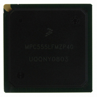
MPC555LFMZP40 Freescale Semiconductor, MPC555LFMZP40 Datasheet - Page 682

MPC555LFMZP40
Manufacturer Part Number
MPC555LFMZP40
Description
IC MCU 32BIT 40MHZ 272-BGA
Manufacturer
Freescale Semiconductor
Series
MPC5xxr
Datasheets
1.MPC555LFMZP40.pdf
(12 pages)
2.MPC555LFMZP40.pdf
(966 pages)
3.MPC555LFMZP40.pdf
(3 pages)
Specifications of MPC555LFMZP40
Core Processor
PowerPC
Core Size
32-Bit
Speed
40MHz
Connectivity
CAN, EBI/EMI, SCI, SPI, UART/USART
Peripherals
POR, PWM, WDT
Number Of I /o
101
Program Memory Size
448KB (448K x 8)
Program Memory Type
FLASH
Ram Size
26K x 8
Voltage - Supply (vcc/vdd)
2.5 V ~ 2.7 V
Data Converters
A/D 32x10b
Oscillator Type
External
Operating Temperature
-40°C ~ 125°C
Package / Case
272-PBGA
Controller Family/series
POWER 5xx
Ram Memory Size
26KB
Cpu Speed
63MIPS
Embedded Interface Type
QSPI, SCI, TouCAN
Operating Temperature Range
-40°C To +125°C
No. Of Pins
272
Rohs Compliant
No
Processor Series
MPC5xx
Core
PowerPC
Data Bus Width
32 bit
Data Ram Size
26 KB
Interface Type
CAN, QSPI, SCI
Maximum Clock Frequency
40 MHz
Number Of Programmable I/os
101
Operating Supply Voltage
3.3 V to 5 V
Maximum Operating Temperature
+ 125 C
Mounting Style
SMD/SMT
Development Tools By Supplier
MPC555CMEE
Minimum Operating Temperature
- 85 C
On-chip Adc
10 bit, 32 Channel
Cpu Family
MPC55xx
Device Core
PowerPC
Device Core Size
32b
Frequency (max)
40MHz
Total Internal Ram Size
32KB
# I/os (max)
101
Operating Supply Voltage (typ)
5V
Instruction Set Architecture
RISC
Operating Temp Range
-40C to 85C
Operating Temperature Classification
Industrial
Mounting
Surface Mount
Pin Count
272
Package Type
BGA
For Use With
MPC555CMEE - KIT EVAL FOR MPC555
Lead Free Status / RoHS Status
Contains lead / RoHS non-compliant
Eeprom Size
-
Lead Free Status / Rohs Status
No
Available stocks
Company
Part Number
Manufacturer
Quantity
Price
Company:
Part Number:
MPC555LFMZP40
Manufacturer:
MOTOLOLA
Quantity:
853
Company:
Part Number:
MPC555LFMZP40
Manufacturer:
Freescale Semiconductor
Quantity:
10 000
Company:
Part Number:
MPC555LFMZP40R2
Manufacturer:
Freescale Semiconductor
Quantity:
10 000
- Current page: 682 of 966
- Download datasheet (15Mb)
19.7.7 Starting and Ending a Program or Erase Sequence
MPC555
USER’S MANUAL
In this example system clock frequency = 40 MHz; the system clock period is therefore
25 ns.
The SES bit is used to signal the start and end of a program or erase sequence. At the
start of a program or erase sequence, SES is set (written to a one). This locks
PROTECT[0:7], SCLKR[0:2], CLKPE[0:1], CLKPM[0:6], BLOCK[0:7], CSC and PE. If
PE = 0 and SES = 1, SIE is write-locked. At this point the CMF EEPROM is ready to
receive either the programming writes or the erase interlock write.
If the PE bit is a zero, the CMF BIU accepts programming writes to the CMF array ad-
dress for programming. The first programming write selects the program page offset
address (ADDR[17:25]) to be programmed along with the data for the programming
buffers at the location written. All programming writes after the first will update the pro-
gram buffers using the lower address (ADDR[26:29]) and the block address (AD-
DR[14:16]) to select the program page buffers to receive the data. For further
information see section
ten to the program buffers the EHV bit is set (written to a one) to start the programming
pulse and lock out further programming writes.
If the PE bit = 1, the CMF BIU accepts writes to any CMF array address as an erase-
interlock write. An erase interlock write is required before the EHV bit can be set.
At the end of the program or erase operation the SES bit must be cleared (written to a
zero) to return to normal operation and release the program buffers, PROTECT[0:7],
SCLKR[0:2], CLKPE[0:1], CLKPM[0:6], BLOCK[0:7], CSC and PE.
The default reset state of SES is not configured for program or erase operation (SES
= 0).
1. Determine SCLKR:
2. Determine CLKPE:
3. Determine CLKPM:
4. Check the results:
/
MPC556
From
From
ponents in the range of N = 5, 6, 7, or 8. While any of these values can be se-
lected CLKPE[0:1] = 0b00, N = 5, will be used for the example.
Using the selected values of N and R in the pulse width equation and solving
for M yields M = 8. Therefore, CLKPM[0:6] = 0x7 (0b0000111).
Pulse Width = System Clock Period
Using SCLKR[0:2] = 0b101, CLKPE[0:1] = 0b00, CLKPM[0:6] = 0b0000111
and PE = 0 at 40 MHz system clock. Pulse Width = 25 ns • 4 • 2
program pulse.
The erase interlock write is a write to any CMF EEPROM array loca-
tion after SES is set and PE = 1.
Table 19-12
Table 19-13
Freescale Semiconductor, Inc.
For More Information On This Product,
19.2.2.2 Program Page
a 40 MHz system clock uses SCLKR[0:2] = 0b101, R = 4.
a 25.6 µs program pulse, PE = 0, can be generated by ex-
CDR MoneT FLASH EEPROM
Go to: www.freescale.com
Rev. 15 October 2000
NOTE
•
R
•
Buffers. After the data has been writ-
2
N
•
M
5
• 8 = 25.6 µs
MOTOROLA
19-30
Related parts for MPC555LFMZP40
Image
Part Number
Description
Manufacturer
Datasheet
Request
R
Part Number:
Description:
Manufacturer:
Freescale Semiconductor, Inc
Datasheet:
Part Number:
Description:
Manufacturer:
Freescale Semiconductor, Inc
Datasheet:
Part Number:
Description:
Manufacturer:
Freescale Semiconductor, Inc
Datasheet:
Part Number:
Description:
Manufacturer:
Freescale Semiconductor, Inc
Datasheet:
Part Number:
Description:
Manufacturer:
Freescale Semiconductor, Inc
Datasheet:
Part Number:
Description:
Manufacturer:
Freescale Semiconductor, Inc
Datasheet:
Part Number:
Description:
Manufacturer:
Freescale Semiconductor, Inc
Datasheet:
Part Number:
Description:
Manufacturer:
Freescale Semiconductor, Inc
Datasheet:
Part Number:
Description:
Manufacturer:
Freescale Semiconductor, Inc
Datasheet:
Part Number:
Description:
Manufacturer:
Freescale Semiconductor, Inc
Datasheet:
Part Number:
Description:
Manufacturer:
Freescale Semiconductor, Inc
Datasheet:
Part Number:
Description:
Manufacturer:
Freescale Semiconductor, Inc
Datasheet:
Part Number:
Description:
Manufacturer:
Freescale Semiconductor, Inc
Datasheet:
Part Number:
Description:
Manufacturer:
Freescale Semiconductor, Inc
Datasheet:
Part Number:
Description:
Manufacturer:
Freescale Semiconductor, Inc
Datasheet:


