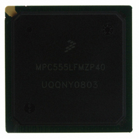
MPC555LFMZP40 Freescale Semiconductor, MPC555LFMZP40 Datasheet - Page 74

MPC555LFMZP40
Manufacturer Part Number
MPC555LFMZP40
Description
IC MCU 32BIT 40MHZ 272-BGA
Manufacturer
Freescale Semiconductor
Series
MPC5xxr
Datasheets
1.MPC555LFMZP40.pdf
(12 pages)
2.MPC555LFMZP40.pdf
(966 pages)
3.MPC555LFMZP40.pdf
(3 pages)
Specifications of MPC555LFMZP40
Core Processor
PowerPC
Core Size
32-Bit
Speed
40MHz
Connectivity
CAN, EBI/EMI, SCI, SPI, UART/USART
Peripherals
POR, PWM, WDT
Number Of I /o
101
Program Memory Size
448KB (448K x 8)
Program Memory Type
FLASH
Ram Size
26K x 8
Voltage - Supply (vcc/vdd)
2.5 V ~ 2.7 V
Data Converters
A/D 32x10b
Oscillator Type
External
Operating Temperature
-40°C ~ 125°C
Package / Case
272-PBGA
Controller Family/series
POWER 5xx
Ram Memory Size
26KB
Cpu Speed
63MIPS
Embedded Interface Type
QSPI, SCI, TouCAN
Operating Temperature Range
-40°C To +125°C
No. Of Pins
272
Rohs Compliant
No
Processor Series
MPC5xx
Core
PowerPC
Data Bus Width
32 bit
Data Ram Size
26 KB
Interface Type
CAN, QSPI, SCI
Maximum Clock Frequency
40 MHz
Number Of Programmable I/os
101
Operating Supply Voltage
3.3 V to 5 V
Maximum Operating Temperature
+ 125 C
Mounting Style
SMD/SMT
Development Tools By Supplier
MPC555CMEE
Minimum Operating Temperature
- 85 C
On-chip Adc
10 bit, 32 Channel
Cpu Family
MPC55xx
Device Core
PowerPC
Device Core Size
32b
Frequency (max)
40MHz
Total Internal Ram Size
32KB
# I/os (max)
101
Operating Supply Voltage (typ)
5V
Instruction Set Architecture
RISC
Operating Temp Range
-40C to 85C
Operating Temperature Classification
Industrial
Mounting
Surface Mount
Pin Count
272
Package Type
BGA
For Use With
MPC555CMEE - KIT EVAL FOR MPC555
Lead Free Status / RoHS Status
Contains lead / RoHS non-compliant
Eeprom Size
-
Lead Free Status / Rohs Status
No
Available stocks
Company
Part Number
Manufacturer
Quantity
Price
Company:
Part Number:
MPC555LFMZP40
Manufacturer:
MOTOLOLA
Quantity:
853
Company:
Part Number:
MPC555LFMZP40
Manufacturer:
Freescale Semiconductor
Quantity:
10 000
Company:
Part Number:
MPC555LFMZP40R2
Manufacturer:
Freescale Semiconductor
Quantity:
10 000
- Current page: 74 of 966
- Download datasheet (15Mb)
2.3.1.17 RSTCONF/TEXP
2.3.1.18 OE
2.3.1.19 BI/STS
2.3.1.20 CS[0:3]
MPC555
USER’S MANUAL
Transfer Error Acknowledge – This signal indicates that a bus error occurred in the
current transaction. The MCU asserts this signal when the bus monitor does not detect
a bus cycle termination within a reasonable amount of time. The assertion of TEA
causes the termination of the current bus cycle, regardless of the state of TEA. An ex-
ternal pull-up device is required to negate TEA quickly, before a second error is de-
tected. That is, the pin must be pulled up within one clock cycle of the time it was three-
stated by the MPC555 / MPC556.
Pin Name: rstconf_b_texp
Reset Configuration – Input. This input line is sampled by the chip during the asser-
tion of the HRESET signal in order to sample the reset configuration. If the line is as-
serted, the configuration mode will be sampled from the external data bus. When this
line is negated, the configuration mode adopted by the chip will be the default one.
Timer Expired – This output line reflects the status of the TEXPS bit in the PLPRCR
register in the USIU. This indicates an expired timer value.
Pin Name: oe_b
Output Enable – This output line is asserted when a read access to an external slave
controlled by the GPCM in the memory controller is initiated by the chip.
Pin Name: bi_b_sts_b
Burst Inhibit – This bi-directional, active low, three-state line indicates that the slave
device addressed in the current burst transaction is not able to support burst transfers.
When the chip drives out the signal for a specific transaction, it asserts or negates BI
during the transaction according to the value specified by the user in the appropriate
control registers. Negation of the signal occurs after the end of the transaction followed
by the immediate three-state. This pin is an active negate signal and may need an ex-
ternal pull-up resistor to ensure proper operation and signal timing specifications.
Special Transfer Start – This output signal is driven by the chip to indicate the start
of a transaction on the external bus or signals the beginning of an internal transaction
in showcycle mode.
Pin Name: cs0_b - cs3_b (4 pins)
Chip Select – These output signals enable peripheral or memory devices at pro-
grammed addresses if defined appropriately in the memory controller. CS0 can be
configured to be the global chip select for the boot device.
/
MPC556
Freescale Semiconductor, Inc.
For More Information On This Product,
Go to: www.freescale.com
SIGNAL DESCRIPTIONS
Rev. 15 October 2000
MOTOROLA
2-16
Related parts for MPC555LFMZP40
Image
Part Number
Description
Manufacturer
Datasheet
Request
R
Part Number:
Description:
Manufacturer:
Freescale Semiconductor, Inc
Datasheet:
Part Number:
Description:
Manufacturer:
Freescale Semiconductor, Inc
Datasheet:
Part Number:
Description:
Manufacturer:
Freescale Semiconductor, Inc
Datasheet:
Part Number:
Description:
Manufacturer:
Freescale Semiconductor, Inc
Datasheet:
Part Number:
Description:
Manufacturer:
Freescale Semiconductor, Inc
Datasheet:
Part Number:
Description:
Manufacturer:
Freescale Semiconductor, Inc
Datasheet:
Part Number:
Description:
Manufacturer:
Freescale Semiconductor, Inc
Datasheet:
Part Number:
Description:
Manufacturer:
Freescale Semiconductor, Inc
Datasheet:
Part Number:
Description:
Manufacturer:
Freescale Semiconductor, Inc
Datasheet:
Part Number:
Description:
Manufacturer:
Freescale Semiconductor, Inc
Datasheet:
Part Number:
Description:
Manufacturer:
Freescale Semiconductor, Inc
Datasheet:
Part Number:
Description:
Manufacturer:
Freescale Semiconductor, Inc
Datasheet:
Part Number:
Description:
Manufacturer:
Freescale Semiconductor, Inc
Datasheet:
Part Number:
Description:
Manufacturer:
Freescale Semiconductor, Inc
Datasheet:
Part Number:
Description:
Manufacturer:
Freescale Semiconductor, Inc
Datasheet:


