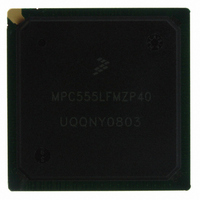
MPC555LFMZP40 Freescale Semiconductor, MPC555LFMZP40 Datasheet - Page 649

MPC555LFMZP40
Manufacturer Part Number
MPC555LFMZP40
Description
IC MCU 32BIT 40MHZ 272-BGA
Manufacturer
Freescale Semiconductor
Series
MPC5xxr
Datasheets
1.MPC555LFMZP40.pdf
(12 pages)
2.MPC555LFMZP40.pdf
(966 pages)
3.MPC555LFMZP40.pdf
(3 pages)
Specifications of MPC555LFMZP40
Core Processor
PowerPC
Core Size
32-Bit
Speed
40MHz
Connectivity
CAN, EBI/EMI, SCI, SPI, UART/USART
Peripherals
POR, PWM, WDT
Number Of I /o
101
Program Memory Size
448KB (448K x 8)
Program Memory Type
FLASH
Ram Size
26K x 8
Voltage - Supply (vcc/vdd)
2.5 V ~ 2.7 V
Data Converters
A/D 32x10b
Oscillator Type
External
Operating Temperature
-40°C ~ 125°C
Package / Case
272-PBGA
Controller Family/series
POWER 5xx
Ram Memory Size
26KB
Cpu Speed
63MIPS
Embedded Interface Type
QSPI, SCI, TouCAN
Operating Temperature Range
-40°C To +125°C
No. Of Pins
272
Rohs Compliant
No
Processor Series
MPC5xx
Core
PowerPC
Data Bus Width
32 bit
Data Ram Size
26 KB
Interface Type
CAN, QSPI, SCI
Maximum Clock Frequency
40 MHz
Number Of Programmable I/os
101
Operating Supply Voltage
3.3 V to 5 V
Maximum Operating Temperature
+ 125 C
Mounting Style
SMD/SMT
Development Tools By Supplier
MPC555CMEE
Minimum Operating Temperature
- 85 C
On-chip Adc
10 bit, 32 Channel
Cpu Family
MPC55xx
Device Core
PowerPC
Device Core Size
32b
Frequency (max)
40MHz
Total Internal Ram Size
32KB
# I/os (max)
101
Operating Supply Voltage (typ)
5V
Instruction Set Architecture
RISC
Operating Temp Range
-40C to 85C
Operating Temperature Classification
Industrial
Mounting
Surface Mount
Pin Count
272
Package Type
BGA
For Use With
MPC555CMEE - KIT EVAL FOR MPC555
Lead Free Status / RoHS Status
Contains lead / RoHS non-compliant
Eeprom Size
-
Lead Free Status / Rohs Status
No
Available stocks
Company
Part Number
Manufacturer
Quantity
Price
Company:
Part Number:
MPC555LFMZP40
Manufacturer:
MOTOLOLA
Quantity:
853
Company:
Part Number:
MPC555LFMZP40
Manufacturer:
Freescale Semiconductor
Quantity:
10 000
Company:
Part Number:
MPC555LFMZP40R2
Manufacturer:
Freescale Semiconductor
Quantity:
10 000
- Current page: 649 of 966
- Download datasheet (15Mb)
18.4.3 Reset Operation
18.4.4 Stop Operation
MPC555
USER’S MANUAL
In order to guarantee valid DPTRAM data during power-down, external low voltage in-
hibit circuitry (external to the MCU) must be designed to force the RESET pin of the
MCU into the active state before VDDL drops below its normal limit. This is necessary
to inhibit spurious writes to the DPTRAM during power-down.
When a synchronous reset occurs, a bus master is allowed to complete the current
access. Thus a write bus cycle (byte or half word) that is in progress when a synchro-
nous reset occurs will be completed without error. Once a write already in progress
has been completed, further writes to the RAM array are inhibited.
If a reset is generated by an asynchronous reset such as the loss of clocks or software
watchdog time-out, the contents of the RAM array are not guaranteed. (Refer to
TION 7 RESET
trol, and status.)
Reset will also reconfigure some of the fields and bits in the DPTRAM control registers
to their default reset state. See the description of the control registers to determine the
effect of reset on these registers.
Setting the STOP control bit in the DPTMCR causes the module to enter its lowest
power-consuming state. The DPTMCR can still be written to allow the STOP control
bit to be cleared.
In stop mode, the DPTRAM array cannot be read or written. All data in the array is re-
tained. The BIU continues to operate to allow the CPU to access the STOP bit in the
DPTMCR. The system clock remains stopped until the STOP bit is cleared or the DP-
TRAM module is reset.
The STOP bit is initialized to logical zero during reset. Only the STOP bit in the DPT-
MCR can be accessed while the STOP bit is asserted. Accesses to other DPTRAM
registers may result in unpredictable behavior. Note also that the STOP bit should be
set and cleared independently of the other control bits in this register to guarantee
proper operation. Changing the state of other bits while changing the state of the
STOP bit may result in unpredictable behavior.
/
MPC556
A word (32-bit) write will be completed coherently only if the reset oc-
curs during the second (16-bit) write bus cycle. If reset occurs during
the first write bus cycle, only the first half word will be written to the
RAM array and the second write will not be allowed to occur. In this
case, the word data contained in the DPTRAM will not be coherent.
The first half word will contain the most significant half of the new
word information and the second half word will contain the least sig-
nificant half of the old word information.
for a description of MPC555 / MPC556 reset sources, operation, con-
Freescale Semiconductor, Inc.
For More Information On This Product,
DUAL-PORT TPU RAM (DPTRAM)
Go to: www.freescale.com
Rev. 15 October 2000
NOTE
MOTOROLA
SEC-
18-7
Related parts for MPC555LFMZP40
Image
Part Number
Description
Manufacturer
Datasheet
Request
R
Part Number:
Description:
Manufacturer:
Freescale Semiconductor, Inc
Datasheet:
Part Number:
Description:
Manufacturer:
Freescale Semiconductor, Inc
Datasheet:
Part Number:
Description:
Manufacturer:
Freescale Semiconductor, Inc
Datasheet:
Part Number:
Description:
Manufacturer:
Freescale Semiconductor, Inc
Datasheet:
Part Number:
Description:
Manufacturer:
Freescale Semiconductor, Inc
Datasheet:
Part Number:
Description:
Manufacturer:
Freescale Semiconductor, Inc
Datasheet:
Part Number:
Description:
Manufacturer:
Freescale Semiconductor, Inc
Datasheet:
Part Number:
Description:
Manufacturer:
Freescale Semiconductor, Inc
Datasheet:
Part Number:
Description:
Manufacturer:
Freescale Semiconductor, Inc
Datasheet:
Part Number:
Description:
Manufacturer:
Freescale Semiconductor, Inc
Datasheet:
Part Number:
Description:
Manufacturer:
Freescale Semiconductor, Inc
Datasheet:
Part Number:
Description:
Manufacturer:
Freescale Semiconductor, Inc
Datasheet:
Part Number:
Description:
Manufacturer:
Freescale Semiconductor, Inc
Datasheet:
Part Number:
Description:
Manufacturer:
Freescale Semiconductor, Inc
Datasheet:
Part Number:
Description:
Manufacturer:
Freescale Semiconductor, Inc
Datasheet:


