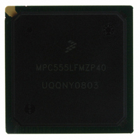
MPC555LFMZP40 Freescale Semiconductor, MPC555LFMZP40 Datasheet - Page 96

MPC555LFMZP40
Manufacturer Part Number
MPC555LFMZP40
Description
IC MCU 32BIT 40MHZ 272-BGA
Manufacturer
Freescale Semiconductor
Series
MPC5xxr
Datasheets
1.MPC555LFMZP40.pdf
(12 pages)
2.MPC555LFMZP40.pdf
(966 pages)
3.MPC555LFMZP40.pdf
(3 pages)
Specifications of MPC555LFMZP40
Core Processor
PowerPC
Core Size
32-Bit
Speed
40MHz
Connectivity
CAN, EBI/EMI, SCI, SPI, UART/USART
Peripherals
POR, PWM, WDT
Number Of I /o
101
Program Memory Size
448KB (448K x 8)
Program Memory Type
FLASH
Ram Size
26K x 8
Voltage - Supply (vcc/vdd)
2.5 V ~ 2.7 V
Data Converters
A/D 32x10b
Oscillator Type
External
Operating Temperature
-40°C ~ 125°C
Package / Case
272-PBGA
Controller Family/series
POWER 5xx
Ram Memory Size
26KB
Cpu Speed
63MIPS
Embedded Interface Type
QSPI, SCI, TouCAN
Operating Temperature Range
-40°C To +125°C
No. Of Pins
272
Rohs Compliant
No
Processor Series
MPC5xx
Core
PowerPC
Data Bus Width
32 bit
Data Ram Size
26 KB
Interface Type
CAN, QSPI, SCI
Maximum Clock Frequency
40 MHz
Number Of Programmable I/os
101
Operating Supply Voltage
3.3 V to 5 V
Maximum Operating Temperature
+ 125 C
Mounting Style
SMD/SMT
Development Tools By Supplier
MPC555CMEE
Minimum Operating Temperature
- 85 C
On-chip Adc
10 bit, 32 Channel
Cpu Family
MPC55xx
Device Core
PowerPC
Device Core Size
32b
Frequency (max)
40MHz
Total Internal Ram Size
32KB
# I/os (max)
101
Operating Supply Voltage (typ)
5V
Instruction Set Architecture
RISC
Operating Temp Range
-40C to 85C
Operating Temperature Classification
Industrial
Mounting
Surface Mount
Pin Count
272
Package Type
BGA
For Use With
MPC555CMEE - KIT EVAL FOR MPC555
Lead Free Status / RoHS Status
Contains lead / RoHS non-compliant
Eeprom Size
-
Lead Free Status / Rohs Status
No
Available stocks
Company
Part Number
Manufacturer
Quantity
Price
Company:
Part Number:
MPC555LFMZP40
Manufacturer:
MOTOLOLA
Quantity:
853
Company:
Part Number:
MPC555LFMZP40
Manufacturer:
Freescale Semiconductor
Quantity:
10 000
Company:
Part Number:
MPC555LFMZP40R2
Manufacturer:
Freescale Semiconductor
Quantity:
10 000
- Current page: 96 of 966
- Download datasheet (15Mb)
2.5.2 Three-Volt Output Pad
2.5.2.1 Type A Interface
MPC555
USER’S MANUAL
These interface signals are referred to in the following pad descriptions and shown in
the pad diagrams.
The output driver of a 3-V output-only pad can be configured to drive a 25-pF or 50-pF
load. There are two subtypes: one with a pull-up device and the other with a pull-down
device. The SPRDS and OE signals enable the pull-up and pull-down resistors.
This pad has a pull-up device to 3 V which can be conditionally turned off based on the
value placed on OE. For a totem pole (push pull) pin with no three-state drive time, the
OE can be connected to VDD, indicating a continuous drive. For a continuous drive,
the pull-up can be disabled.
• Drive select – Selects the drive strength of the pad. For example, data pin drivers
• Synchronizer clock – Some pins have synchronizer logic to handle metastable
• Slew rate control – GPIO pins have slow slew rates, with edge rates in the range
• Hysteresis input – Slow pads contains hysteresis input buffers to reduce the sen-
• Open drain enable – For selected 3-V / 5-V pads, this signal determines the type
• Pull resistor disable select (PRDS) – Reflects the state of the PRDS bit in the pad
• Special pull resistor disable select (SPRDS) – Reflects the state of the SPRDS
• Analog – Analog input signals to the QADC. The corresponding digital interface
• JTAG – Joint Test Access Group related signals that are used for connectivity
/
can be configured to drive a 25-pF load or a 50-pF load.
signals at the input of a pin. For pads that have synchronizers and support syn-
chronized or normal data input, the corresponding interface signals to the internal
logic are “Normal Data In” and “Sync Data In.”
of 90 ns to 600 ns. The slew rate and weak pull-up/pull-down characteristics of
these pins are controlled by bits in the PDMCR, see
ration Register
controllable slew rates, see
sitivity to noises. The input hyst_sel is used to configure the pad to provide hys-
teresis according to the pad configuration.
of drive (open drain or totem pole) seen at the pin.
module configuration register (PDMCR). This signal controls the pull-up/pull-
down resistor for the SGPIO pins and the pins for the modules on the UIMB.
bit in the PDMCR. For pins that support bus arbitration functionality multiplexed
with opcode-tracking and debug functionality, this signal controls the pull-up re-
sistors.
signals are referred to as “Dig. In” and Dig. Out”.
tests at the board level. These signals are not shown in the pad block diagrams
in this section. In addition, the effect of the pull-up/pull-down resistors is not illus-
trated in the pad block diagrams.
MPC556
Freescale Semiconductor, Inc.
(PDMCR). For a description of PDMCR bits SLRC[0:3] that have
For More Information On This Product,
Go to: www.freescale.com
SIGNAL DESCRIPTIONS
Rev. 15 October 2000
Table
2-3.
2.4.2 Pad Module Configu-
MOTOROLA
2-38
Related parts for MPC555LFMZP40
Image
Part Number
Description
Manufacturer
Datasheet
Request
R
Part Number:
Description:
Manufacturer:
Freescale Semiconductor, Inc
Datasheet:
Part Number:
Description:
Manufacturer:
Freescale Semiconductor, Inc
Datasheet:
Part Number:
Description:
Manufacturer:
Freescale Semiconductor, Inc
Datasheet:
Part Number:
Description:
Manufacturer:
Freescale Semiconductor, Inc
Datasheet:
Part Number:
Description:
Manufacturer:
Freescale Semiconductor, Inc
Datasheet:
Part Number:
Description:
Manufacturer:
Freescale Semiconductor, Inc
Datasheet:
Part Number:
Description:
Manufacturer:
Freescale Semiconductor, Inc
Datasheet:
Part Number:
Description:
Manufacturer:
Freescale Semiconductor, Inc
Datasheet:
Part Number:
Description:
Manufacturer:
Freescale Semiconductor, Inc
Datasheet:
Part Number:
Description:
Manufacturer:
Freescale Semiconductor, Inc
Datasheet:
Part Number:
Description:
Manufacturer:
Freescale Semiconductor, Inc
Datasheet:
Part Number:
Description:
Manufacturer:
Freescale Semiconductor, Inc
Datasheet:
Part Number:
Description:
Manufacturer:
Freescale Semiconductor, Inc
Datasheet:
Part Number:
Description:
Manufacturer:
Freescale Semiconductor, Inc
Datasheet:
Part Number:
Description:
Manufacturer:
Freescale Semiconductor, Inc
Datasheet:


