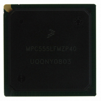
MPC555LFMZP40 Freescale Semiconductor, MPC555LFMZP40 Datasheet - Page 655

MPC555LFMZP40
Manufacturer Part Number
MPC555LFMZP40
Description
IC MCU 32BIT 40MHZ 272-BGA
Manufacturer
Freescale Semiconductor
Series
MPC5xxr
Datasheets
1.MPC555LFMZP40.pdf
(12 pages)
2.MPC555LFMZP40.pdf
(966 pages)
3.MPC555LFMZP40.pdf
(3 pages)
Specifications of MPC555LFMZP40
Core Processor
PowerPC
Core Size
32-Bit
Speed
40MHz
Connectivity
CAN, EBI/EMI, SCI, SPI, UART/USART
Peripherals
POR, PWM, WDT
Number Of I /o
101
Program Memory Size
448KB (448K x 8)
Program Memory Type
FLASH
Ram Size
26K x 8
Voltage - Supply (vcc/vdd)
2.5 V ~ 2.7 V
Data Converters
A/D 32x10b
Oscillator Type
External
Operating Temperature
-40°C ~ 125°C
Package / Case
272-PBGA
Controller Family/series
POWER 5xx
Ram Memory Size
26KB
Cpu Speed
63MIPS
Embedded Interface Type
QSPI, SCI, TouCAN
Operating Temperature Range
-40°C To +125°C
No. Of Pins
272
Rohs Compliant
No
Processor Series
MPC5xx
Core
PowerPC
Data Bus Width
32 bit
Data Ram Size
26 KB
Interface Type
CAN, QSPI, SCI
Maximum Clock Frequency
40 MHz
Number Of Programmable I/os
101
Operating Supply Voltage
3.3 V to 5 V
Maximum Operating Temperature
+ 125 C
Mounting Style
SMD/SMT
Development Tools By Supplier
MPC555CMEE
Minimum Operating Temperature
- 85 C
On-chip Adc
10 bit, 32 Channel
Cpu Family
MPC55xx
Device Core
PowerPC
Device Core Size
32b
Frequency (max)
40MHz
Total Internal Ram Size
32KB
# I/os (max)
101
Operating Supply Voltage (typ)
5V
Instruction Set Architecture
RISC
Operating Temp Range
-40C to 85C
Operating Temperature Classification
Industrial
Mounting
Surface Mount
Pin Count
272
Package Type
BGA
For Use With
MPC555CMEE - KIT EVAL FOR MPC555
Lead Free Status / RoHS Status
Contains lead / RoHS non-compliant
Eeprom Size
-
Lead Free Status / Rohs Status
No
Available stocks
Company
Part Number
Manufacturer
Quantity
Price
Company:
Part Number:
MPC555LFMZP40
Manufacturer:
MOTOLOLA
Quantity:
853
Company:
Part Number:
MPC555LFMZP40
Manufacturer:
Freescale Semiconductor
Quantity:
10 000
Company:
Part Number:
MPC555LFMZP40R2
Manufacturer:
Freescale Semiconductor
Quantity:
10 000
- Current page: 655 of 966
- Download datasheet (15Mb)
MPC555
USER’S MANUAL
• Erase interlock write — A write to any CMF array address after initializing the
• Erase margin read — Special off-page read of the CMF array where the CMF
• Information censorship — CENSOR[0:1] = 11. Requires an erase of the CMF
• Initialize program/erase sequence — The write to the high voltage control reg-
• MoneT — The CMF EEPROM’s FLASH bit cell.
• No censorship — CENSOR[0:1] = 10 or 01, The CMF EEPROM can change to
• Off-page read — Array read operation that requires two clocks and updates a
• On-page read — Array read operation that accesses information in one of the
• Over-programmed — By exceeding the specified programming time and/or volt-
• Programming write — A word write to a CMF array address to transfer informa-
• Program margin read — Special off-page read of the CMF array where the CMF
• Program page buffer — 64 bytes of information used to program the CMF array.
• Read page buffer — 32-byte block of information that is read from the CMF ar-
• Shadow information — An extra row (256 bytes) of the CMF array used to pro-
/
either no censorship or information censorship without modifying the CMF array
contents. Cleared censorship will prevent CMF array accesses when the device
is censored and ACCESS = 0.
erase sequence.
EEPROM hardware adjusts the reference of the sense amplifier to check for cor-
rect erase operation. All CMF array off-page read accesses between the erase
interlock write and clearing the SES bit are erase margin reads.
EEPROM to change CENSOR[0:1]. Information censorship will prevent CMF ar-
ray accesses when the device is censored and ACCESS = 0. Information stored
in the CMF array is made invalid while clearing CENSOR[0:1].
ister that changes the SES bit from a zero to a one.
information censorship without modifying the CMF array contents. No censorship
allows all CMF array accesses.
page buffer.
read page buffers and requires one clock.
age a CMF bit may be over-programmed. This bit will cause erased bits on the
same column in the same array block to read as programmed.
tion into a program page buffer. The CMF EEPROM accepts programming writes
from after initializing the program sequence until the EHV bit is changed from a
zero to a one.
EEPROM hardware adjusts the reference of the sense amplifier to check for cor-
rect program operation. All CMF array off-page read accesses between the first
programming write and clearing the SES bit are program margin reads.
This information is aligned to a 64-byte boundary within the CMF array block.
Each CMF module has one program page buffer for each array block.
ray. This information is aligned to a 32-byte boundary within the CMF array. Each
CMF module has two read page buffers.
vide reset configuration information. This row may be accessed by setting the SIE
bit in the module configuration register and accessing the CMF array. The shad-
ow information is always in the lowest array block of the CMF array.
MPC556
Freescale Semiconductor, Inc.
For More Information On This Product,
CDR MoneT FLASH EEPROM
Go to: www.freescale.com
Rev. 15 October 2000
MOTOROLA
19-3
Related parts for MPC555LFMZP40
Image
Part Number
Description
Manufacturer
Datasheet
Request
R
Part Number:
Description:
Manufacturer:
Freescale Semiconductor, Inc
Datasheet:
Part Number:
Description:
Manufacturer:
Freescale Semiconductor, Inc
Datasheet:
Part Number:
Description:
Manufacturer:
Freescale Semiconductor, Inc
Datasheet:
Part Number:
Description:
Manufacturer:
Freescale Semiconductor, Inc
Datasheet:
Part Number:
Description:
Manufacturer:
Freescale Semiconductor, Inc
Datasheet:
Part Number:
Description:
Manufacturer:
Freescale Semiconductor, Inc
Datasheet:
Part Number:
Description:
Manufacturer:
Freescale Semiconductor, Inc
Datasheet:
Part Number:
Description:
Manufacturer:
Freescale Semiconductor, Inc
Datasheet:
Part Number:
Description:
Manufacturer:
Freescale Semiconductor, Inc
Datasheet:
Part Number:
Description:
Manufacturer:
Freescale Semiconductor, Inc
Datasheet:
Part Number:
Description:
Manufacturer:
Freescale Semiconductor, Inc
Datasheet:
Part Number:
Description:
Manufacturer:
Freescale Semiconductor, Inc
Datasheet:
Part Number:
Description:
Manufacturer:
Freescale Semiconductor, Inc
Datasheet:
Part Number:
Description:
Manufacturer:
Freescale Semiconductor, Inc
Datasheet:
Part Number:
Description:
Manufacturer:
Freescale Semiconductor, Inc
Datasheet:


