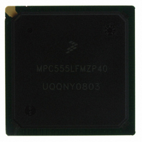
MPC555LFMZP40 Freescale Semiconductor, MPC555LFMZP40 Datasheet - Page 512

MPC555LFMZP40
Manufacturer Part Number
MPC555LFMZP40
Description
IC MCU 32BIT 40MHZ 272-BGA
Manufacturer
Freescale Semiconductor
Series
MPC5xxr
Datasheets
1.MPC555LFMZP40.pdf
(12 pages)
2.MPC555LFMZP40.pdf
(966 pages)
3.MPC555LFMZP40.pdf
(3 pages)
Specifications of MPC555LFMZP40
Core Processor
PowerPC
Core Size
32-Bit
Speed
40MHz
Connectivity
CAN, EBI/EMI, SCI, SPI, UART/USART
Peripherals
POR, PWM, WDT
Number Of I /o
101
Program Memory Size
448KB (448K x 8)
Program Memory Type
FLASH
Ram Size
26K x 8
Voltage - Supply (vcc/vdd)
2.5 V ~ 2.7 V
Data Converters
A/D 32x10b
Oscillator Type
External
Operating Temperature
-40°C ~ 125°C
Package / Case
272-PBGA
Controller Family/series
POWER 5xx
Ram Memory Size
26KB
Cpu Speed
63MIPS
Embedded Interface Type
QSPI, SCI, TouCAN
Operating Temperature Range
-40°C To +125°C
No. Of Pins
272
Rohs Compliant
No
Processor Series
MPC5xx
Core
PowerPC
Data Bus Width
32 bit
Data Ram Size
26 KB
Interface Type
CAN, QSPI, SCI
Maximum Clock Frequency
40 MHz
Number Of Programmable I/os
101
Operating Supply Voltage
3.3 V to 5 V
Maximum Operating Temperature
+ 125 C
Mounting Style
SMD/SMT
Development Tools By Supplier
MPC555CMEE
Minimum Operating Temperature
- 85 C
On-chip Adc
10 bit, 32 Channel
Cpu Family
MPC55xx
Device Core
PowerPC
Device Core Size
32b
Frequency (max)
40MHz
Total Internal Ram Size
32KB
# I/os (max)
101
Operating Supply Voltage (typ)
5V
Instruction Set Architecture
RISC
Operating Temp Range
-40C to 85C
Operating Temperature Classification
Industrial
Mounting
Surface Mount
Pin Count
272
Package Type
BGA
For Use With
MPC555CMEE - KIT EVAL FOR MPC555
Lead Free Status / RoHS Status
Contains lead / RoHS non-compliant
Eeprom Size
-
Lead Free Status / Rohs Status
No
Available stocks
Company
Part Number
Manufacturer
Quantity
Price
Company:
Part Number:
MPC555LFMZP40
Manufacturer:
MOTOLOLA
Quantity:
853
Company:
Part Number:
MPC555LFMZP40
Manufacturer:
Freescale Semiconductor
Quantity:
10 000
Company:
Part Number:
MPC555LFMZP40R2
Manufacturer:
Freescale Semiconductor
Quantity:
10 000
- Current page: 512 of 966
- Download datasheet (15Mb)
14.8.6 SCI Pins
14.8.7 SCI Operation
14.8.7.1 Definition of Terms
MPC555
USER’S MANUAL
Bit(s)
7:15
0:6
The RXD1 and RXD2 pins are the receive data pins for the SCI1 and SCI2, respec-
tively. TXD1 and TXD2 are the transmit data pins for the two SCI modules. An external
clock pin, ECK, is common to both SCIs. The pins and their functions are listed in
ble
The SCI can operate in polled or interrupt-driven mode. Status flags in SCxSR reflect
SCI conditions regardless of the operating mode chosen. The TIE, TCIE, RIE, and ILIE
bits in SCCxR1 enable interrupts for the conditions indicated by the TDRE, TC, RDRF,
and IDLE bits in SCxSR, respectively.
• Bit-time — The time required to transmit or receive one bit of data, which is equal
• Start bit — One bit-time of logic zero that indicates the beginning of a data frame.
• Stop bit— One bit-time of logic one that indicates the end of a data frame.
• Frame — A complete unit of serial information. The SCI can use 10-bit or 11-bit
• Data frame — A start bit, a specified number of data or information bits, and at
• Idle frame — A frame that consists of consecutive ones. An idle frame has no start
External Clock
Transmit Data
14-27.
Receive Data
/
Pin Names
to one cycle of the baud frequency.
A start bit must begin with a one-to-zero transition and be preceded by at least
three receive time samples of logic one.
frames.
least one stop bit.
bit.
R[8:0]/
MPC556
Name
T[8:0]
—
Reserved
R[7:0]/T[7:0] contain either the eight data bits received when SCxDR is read, or the eight data
bits to be transmitted when SCxDR is written. R8/T8 are used when the SCI is configured for
nine-bit operation (M = 1). When the SCI is configured for 8-bit operation, R8/T8 have no mean-
ing or effect.
Accesses to the lower byte of SCxDR triggers the mechanism for clearing the status bits or for
initiating transmissions whether byte, half-word, or word accesses are used.
Freescale Semiconductor, Inc.
QUEUED SERIAL MULTI-CHANNEL MODULE
Table 14-26 SCxSR Bit Descriptions
For More Information On This Product,
RXD1, RXD2
TXD1, TXD2
Mnemonic
Table 14-27 SCI Pin Functions
ECK
Go to: www.freescale.com
Rev. 15 October 2000
Receiver disabled
Receiver enabled
Transmitter disabled
Transmitter enabled
Receiver disabled
Receiver enabled
Transmitter disabled
Transmitter enabled
Mode
Description
General purpose input
Serial data input to SCI
General purpose output
Serial data output from SCI
Not used
Alternate input source to baud
Not used
Alternate input source to baud
Function
MOTOROLA
14-50
Ta-
Related parts for MPC555LFMZP40
Image
Part Number
Description
Manufacturer
Datasheet
Request
R
Part Number:
Description:
Manufacturer:
Freescale Semiconductor, Inc
Datasheet:
Part Number:
Description:
Manufacturer:
Freescale Semiconductor, Inc
Datasheet:
Part Number:
Description:
Manufacturer:
Freescale Semiconductor, Inc
Datasheet:
Part Number:
Description:
Manufacturer:
Freescale Semiconductor, Inc
Datasheet:
Part Number:
Description:
Manufacturer:
Freescale Semiconductor, Inc
Datasheet:
Part Number:
Description:
Manufacturer:
Freescale Semiconductor, Inc
Datasheet:
Part Number:
Description:
Manufacturer:
Freescale Semiconductor, Inc
Datasheet:
Part Number:
Description:
Manufacturer:
Freescale Semiconductor, Inc
Datasheet:
Part Number:
Description:
Manufacturer:
Freescale Semiconductor, Inc
Datasheet:
Part Number:
Description:
Manufacturer:
Freescale Semiconductor, Inc
Datasheet:
Part Number:
Description:
Manufacturer:
Freescale Semiconductor, Inc
Datasheet:
Part Number:
Description:
Manufacturer:
Freescale Semiconductor, Inc
Datasheet:
Part Number:
Description:
Manufacturer:
Freescale Semiconductor, Inc
Datasheet:
Part Number:
Description:
Manufacturer:
Freescale Semiconductor, Inc
Datasheet:
Part Number:
Description:
Manufacturer:
Freescale Semiconductor, Inc
Datasheet:


