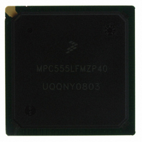
MPC555LFMZP40 Freescale Semiconductor, MPC555LFMZP40 Datasheet - Page 647

MPC555LFMZP40
Manufacturer Part Number
MPC555LFMZP40
Description
IC MCU 32BIT 40MHZ 272-BGA
Manufacturer
Freescale Semiconductor
Series
MPC5xxr
Datasheets
1.MPC555LFMZP40.pdf
(12 pages)
2.MPC555LFMZP40.pdf
(966 pages)
3.MPC555LFMZP40.pdf
(3 pages)
Specifications of MPC555LFMZP40
Core Processor
PowerPC
Core Size
32-Bit
Speed
40MHz
Connectivity
CAN, EBI/EMI, SCI, SPI, UART/USART
Peripherals
POR, PWM, WDT
Number Of I /o
101
Program Memory Size
448KB (448K x 8)
Program Memory Type
FLASH
Ram Size
26K x 8
Voltage - Supply (vcc/vdd)
2.5 V ~ 2.7 V
Data Converters
A/D 32x10b
Oscillator Type
External
Operating Temperature
-40°C ~ 125°C
Package / Case
272-PBGA
Controller Family/series
POWER 5xx
Ram Memory Size
26KB
Cpu Speed
63MIPS
Embedded Interface Type
QSPI, SCI, TouCAN
Operating Temperature Range
-40°C To +125°C
No. Of Pins
272
Rohs Compliant
No
Processor Series
MPC5xx
Core
PowerPC
Data Bus Width
32 bit
Data Ram Size
26 KB
Interface Type
CAN, QSPI, SCI
Maximum Clock Frequency
40 MHz
Number Of Programmable I/os
101
Operating Supply Voltage
3.3 V to 5 V
Maximum Operating Temperature
+ 125 C
Mounting Style
SMD/SMT
Development Tools By Supplier
MPC555CMEE
Minimum Operating Temperature
- 85 C
On-chip Adc
10 bit, 32 Channel
Cpu Family
MPC55xx
Device Core
PowerPC
Device Core Size
32b
Frequency (max)
40MHz
Total Internal Ram Size
32KB
# I/os (max)
101
Operating Supply Voltage (typ)
5V
Instruction Set Architecture
RISC
Operating Temp Range
-40C to 85C
Operating Temperature Classification
Industrial
Mounting
Surface Mount
Pin Count
272
Package Type
BGA
For Use With
MPC555CMEE - KIT EVAL FOR MPC555
Lead Free Status / RoHS Status
Contains lead / RoHS non-compliant
Eeprom Size
-
Lead Free Status / Rohs Status
No
Available stocks
Company
Part Number
Manufacturer
Quantity
Price
Company:
Part Number:
MPC555LFMZP40
Manufacturer:
MOTOLOLA
Quantity:
853
Company:
Part Number:
MPC555LFMZP40
Manufacturer:
Freescale Semiconductor
Quantity:
10 000
Company:
Part Number:
MPC555LFMZP40R2
Manufacturer:
Freescale Semiconductor
Quantity:
10 000
- Current page: 647 of 966
- Download datasheet (15Mb)
RAMBAR — RAM Array Base Address Register
MISRH — Multiple Input Signature Register High
RESET:
18.3.3 Ram Base Address Register (RAMBAR)
18.3.4 MISR High (MISRH) and MISR Low (MISRL)
MPC555
USER’S MANUAL
MSB
MSB
A8
Bit(s)
11:14
0
0
0:10
0
15
The RAMBAR register is used to specify the 16 MSBs of the starting DPT RAM array
location in the memory map. In the MPC555 / MPC556, this register must be pro-
gramed to the value 0xFFA0.
This register can be written only once after a reset. This prevents runaway software
from inadvertently re-mapping the array. Since the locking mechanism is triggered by
the first write after reset, the base address of the array should be written in a single
operation. Writing only one half of the register will prevent the other half from being
written.
Soft reset has no effect on this register.
The MISRH and MISRL together contain the 32-bit RAM signature calculated by the
MISC. These registers are read-only and should be read by the host when the MISF
bit in the MCR is set. Note that the naming of the D[31:0] bits represents little-endian
bit encoding.
Exiting TPU3 emulation mode results in the reset of both MISRH and MISRL
A9
1
0
1
/
RAMDS
A[8:18]
MPC556
Name
—
A10
2
0
2
RAM array base address. These bits specify the 11 high-order bits (address lines ADDR[8:18]
in little-endian notation) of the 24-bit base address of the RAM array. This allows the array to be
placed on a 8-Kbyte boundary anywhere in the memory map. It is the users responsibility not to
overlap the RAM array memory map with other modules on the chip.
On the MPC555 / MPC556 the value 0xFFA0 must be used.
Reserved. (Bits 11:12 represent A[19:20] in DPTRAM implementations that require them.
RAM disabled. RAMDS is a read-only status bit. The RAM array is disabled after a master reset
since the RAMBAR register may be incorrect. When the array is disabled, it will not respond to
any addresses on the IMB3. Access to the RAM control register block is not affected when the
array is disabled.
RAMDS is cleared by the DPTRAM module when a base address is written to the array address
field of RAMBAR.
RAMDS = 0: RAM enabled
RAMDS = 1: RAM disabled
A11
3
0
3
Freescale Semiconductor, Inc.
A12
Table 18-3 RAMBAR Bit Descriptions
4
0
4
For More Information On This Product,
A13
DUAL-PORT TPU RAM (DPTRAM)
5
0
5
Go to: www.freescale.com
Rev. 15 October 2000
A14
6
0
6
A15
7
0
7
A16
8
0
8
Description
A17
9
0
9
A18
10
10
0
11
11
0
12
12
Reserved
0
13
13
0
0x30 0004
0x30 0006
MOTOROLA
14
14
0
RAMDS
18-5
LSB
LSB
15
15
1
Related parts for MPC555LFMZP40
Image
Part Number
Description
Manufacturer
Datasheet
Request
R
Part Number:
Description:
Manufacturer:
Freescale Semiconductor, Inc
Datasheet:
Part Number:
Description:
Manufacturer:
Freescale Semiconductor, Inc
Datasheet:
Part Number:
Description:
Manufacturer:
Freescale Semiconductor, Inc
Datasheet:
Part Number:
Description:
Manufacturer:
Freescale Semiconductor, Inc
Datasheet:
Part Number:
Description:
Manufacturer:
Freescale Semiconductor, Inc
Datasheet:
Part Number:
Description:
Manufacturer:
Freescale Semiconductor, Inc
Datasheet:
Part Number:
Description:
Manufacturer:
Freescale Semiconductor, Inc
Datasheet:
Part Number:
Description:
Manufacturer:
Freescale Semiconductor, Inc
Datasheet:
Part Number:
Description:
Manufacturer:
Freescale Semiconductor, Inc
Datasheet:
Part Number:
Description:
Manufacturer:
Freescale Semiconductor, Inc
Datasheet:
Part Number:
Description:
Manufacturer:
Freescale Semiconductor, Inc
Datasheet:
Part Number:
Description:
Manufacturer:
Freescale Semiconductor, Inc
Datasheet:
Part Number:
Description:
Manufacturer:
Freescale Semiconductor, Inc
Datasheet:
Part Number:
Description:
Manufacturer:
Freescale Semiconductor, Inc
Datasheet:
Part Number:
Description:
Manufacturer:
Freescale Semiconductor, Inc
Datasheet:


