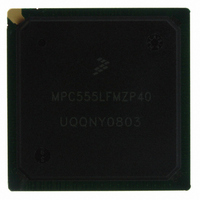
MPC555LFMZP40 Freescale Semiconductor, MPC555LFMZP40 Datasheet - Page 64

MPC555LFMZP40
Manufacturer Part Number
MPC555LFMZP40
Description
IC MCU 32BIT 40MHZ 272-BGA
Manufacturer
Freescale Semiconductor
Series
MPC5xxr
Datasheets
1.MPC555LFMZP40.pdf
(12 pages)
2.MPC555LFMZP40.pdf
(966 pages)
3.MPC555LFMZP40.pdf
(3 pages)
Specifications of MPC555LFMZP40
Core Processor
PowerPC
Core Size
32-Bit
Speed
40MHz
Connectivity
CAN, EBI/EMI, SCI, SPI, UART/USART
Peripherals
POR, PWM, WDT
Number Of I /o
101
Program Memory Size
448KB (448K x 8)
Program Memory Type
FLASH
Ram Size
26K x 8
Voltage - Supply (vcc/vdd)
2.5 V ~ 2.7 V
Data Converters
A/D 32x10b
Oscillator Type
External
Operating Temperature
-40°C ~ 125°C
Package / Case
272-PBGA
Controller Family/series
POWER 5xx
Ram Memory Size
26KB
Cpu Speed
63MIPS
Embedded Interface Type
QSPI, SCI, TouCAN
Operating Temperature Range
-40°C To +125°C
No. Of Pins
272
Rohs Compliant
No
Processor Series
MPC5xx
Core
PowerPC
Data Bus Width
32 bit
Data Ram Size
26 KB
Interface Type
CAN, QSPI, SCI
Maximum Clock Frequency
40 MHz
Number Of Programmable I/os
101
Operating Supply Voltage
3.3 V to 5 V
Maximum Operating Temperature
+ 125 C
Mounting Style
SMD/SMT
Development Tools By Supplier
MPC555CMEE
Minimum Operating Temperature
- 85 C
On-chip Adc
10 bit, 32 Channel
Cpu Family
MPC55xx
Device Core
PowerPC
Device Core Size
32b
Frequency (max)
40MHz
Total Internal Ram Size
32KB
# I/os (max)
101
Operating Supply Voltage (typ)
5V
Instruction Set Architecture
RISC
Operating Temp Range
-40C to 85C
Operating Temperature Classification
Industrial
Mounting
Surface Mount
Pin Count
272
Package Type
BGA
For Use With
MPC555CMEE - KIT EVAL FOR MPC555
Lead Free Status / RoHS Status
Contains lead / RoHS non-compliant
Eeprom Size
-
Lead Free Status / Rohs Status
No
Available stocks
Company
Part Number
Manufacturer
Quantity
Price
Company:
Part Number:
MPC555LFMZP40
Manufacturer:
MOTOLOLA
Quantity:
853
Company:
Part Number:
MPC555LFMZP40
Manufacturer:
Freescale Semiconductor
Quantity:
10 000
Company:
Part Number:
MPC555LFMZP40R2
Manufacturer:
Freescale Semiconductor
Quantity:
10 000
- Current page: 64 of 966
- Download datasheet (15Mb)
2.2 Pin Functionality
MPC555
USER’S MANUAL
NOTES:
1. “/” implies that the corresponding functions are multiplexed on the pin
2. All inputs are 5 V friendly. All 5 V outputs are slow slew rate except for SCI transmit pins.
3. These pins are powered by KAPWR (Keep Alive Power Supply).
The pad ring supports 234 functional pins (284 including all power and ground). Some
pins serve multiple functions. The pad characteristics for each pin are described in
ble
Table 2-1 MPC555 / MPC556 Pin Functions for 272-Pin PBGA (Continued)
Programming Voltage
High voltage Supply
Functional Group
• Pin – List of functional (signal) names for each pin. (For actual pin names, see
• Function – Name of function (signal). Each pin supports one or more functions,
• Driver Type – Type of driver that is used to drive the pin (for output functionality).
• Receiver Type – Type of receiver used for the pin. Some inputs need to have a
• Direction – Direction of the pin for each function it supports. The possible direc-
• Voltage – Voltage requirement for each function of a pin. There are two supply
• Slew rate – Timing needed from the 5-V drivers. The options are with slew rate
• Drive strength – Drive strength for 3-V drivers of the output load. For all 3-V out-
• Pad Type – Functional pad structure used for a pin. For pad type descriptions,
2-2. This table contains the following columns:
/
Pin Names and
and each function (signal) name is a separate entry in the table.
Types of output drivers are:
synchronizer to prevent latching a metastable signal at the pins. Such require-
ments are indicated in this column with the abbreviation “synch.” Another possible
entry is “glitch filter.” It is added to reset signals.
tions are input (I), output (O) and bi-directional (I/O).
voltages: 5 V and 3 V.
(typically 200/50 ns with 50 pF load) or fast 5-V driver.
puts, the drive strength is 25/50 pF. For two pads (clkout and engclk) the drive
strength is 45/90 pF.
see
— Totem pole (TP). This driver type uses a push pull scheme to drive the pin.
— Open drain (OD). This driver type uses an open drain approach to drive the
— Active negated (ANG). This driver type fully drives a low level. A high level is
MPC556
These pins can be driven high or low or can be three-stated. Care must be tak-
en to ensure that there is no contention on this pin (for example, an external
driver driving the pin high while an internal driver is driving it low).
pins. Pins with an OD driver can be either driven low or three-stated. This driver
scheme is typically used for pins that could potentially be asserted by multiple
modules.
driven and then released. A pull-up resistor may be needed on this type of out-
put.
2.5 Pad
Types.
Freescale Semiconductor, Inc.
Abbreviations.
For More Information On This Product,
Go to: www.freescale.com
SIGNAL DESCRIPTIONS
Rev. 15 October 2000
VDDH, VDDA, VRH
Signals
VPP
1
Pins
12
1
MOTOROLA
3 V / 5 V
3-V / 5-V
5 V
Ta-
2
2.7
2-6
Related parts for MPC555LFMZP40
Image
Part Number
Description
Manufacturer
Datasheet
Request
R
Part Number:
Description:
Manufacturer:
Freescale Semiconductor, Inc
Datasheet:
Part Number:
Description:
Manufacturer:
Freescale Semiconductor, Inc
Datasheet:
Part Number:
Description:
Manufacturer:
Freescale Semiconductor, Inc
Datasheet:
Part Number:
Description:
Manufacturer:
Freescale Semiconductor, Inc
Datasheet:
Part Number:
Description:
Manufacturer:
Freescale Semiconductor, Inc
Datasheet:
Part Number:
Description:
Manufacturer:
Freescale Semiconductor, Inc
Datasheet:
Part Number:
Description:
Manufacturer:
Freescale Semiconductor, Inc
Datasheet:
Part Number:
Description:
Manufacturer:
Freescale Semiconductor, Inc
Datasheet:
Part Number:
Description:
Manufacturer:
Freescale Semiconductor, Inc
Datasheet:
Part Number:
Description:
Manufacturer:
Freescale Semiconductor, Inc
Datasheet:
Part Number:
Description:
Manufacturer:
Freescale Semiconductor, Inc
Datasheet:
Part Number:
Description:
Manufacturer:
Freescale Semiconductor, Inc
Datasheet:
Part Number:
Description:
Manufacturer:
Freescale Semiconductor, Inc
Datasheet:
Part Number:
Description:
Manufacturer:
Freescale Semiconductor, Inc
Datasheet:
Part Number:
Description:
Manufacturer:
Freescale Semiconductor, Inc
Datasheet:


