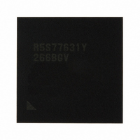
R5S77631Y266BGV Renesas Electronics America, R5S77631Y266BGV Datasheet - Page 1122

R5S77631Y266BGV
Manufacturer Part Number
R5S77631Y266BGV
Description
IC SUPERH MPU ROMLESS 499BGA
Manufacturer
Renesas Electronics America
Series
SuperH® SH7780r
Datasheet
1.R5S77631Y266BGV.pdf
(2056 pages)
Specifications of R5S77631Y266BGV
Core Processor
SH-4A
Core Size
32-Bit
Speed
266MHz
Connectivity
Audio Codec, I²C, MMC, SCI, SIM, SIO, SSI, USB
Peripherals
DMA, LCD, POR, WDT
Number Of I /o
107
Program Memory Type
ROMless
Ram Size
16K x 8
Voltage - Supply (vcc/vdd)
1.15 V ~ 1.35 V
Data Converters
A/D 4x10b; D/A 2x8b
Oscillator Type
External
Operating Temperature
-20°C ~ 75°C
Package / Case
499-BGA
Lead Free Status / RoHS Status
Lead free / RoHS Compliant
Eeprom Size
-
Program Memory Size
-
Available stocks
Company
Part Number
Manufacturer
Quantity
Price
Company:
Part Number:
R5S77631Y266BGV
Manufacturer:
Renesas Electronics America
Quantity:
10 000
- Current page: 1122 of 2056
- Download datasheet (10Mb)
Section 26 I
26.4.8
The transmit procedure and operation in master transmit mode are described below. Figure 26.9
shows the timing chart in master transmit mode. Setting the MDBS bit in the master control
register allows the IIC to operate in single-buffer mode.
1. For initial setting, set the clock control register and the master interrupt enable register
2. Monitor the FSDA bit in the master control register. Confirm that this bit is low, meaning that
3. After the transmit START condition, slave address, and data transfer direction bits are
4. An interrupt due to the SAR bit is generated at the timing of (3) shown in figure 26.9. If the
5. Data is transmitted in units of nine bits: 8-bit data and 1-bit ACK. An interrupt of MDE (bit 3)
6. To end data transfer, an interrupt of MNR (bit 6) in the master status register is generated at
7. The FSB bit needs to be set before the last byte data is transferred. In master transmit mode,
Rev. 2.00 May 22, 2009 Page 1052 of 1982
REJ09B0256-0200
according to the slave address, transmit data, and the transmit speed. Since slave mode is also
required even when master mode is used, set the device address in the slave address register.
other I
bits in the master control register to 1 to start master transmission.
transmitted, an interrupt due to the MAT and MDE bits in the master status register is
generated at the timing of (1) in figure 26.9. At this time, clear the ESG bit to 0. To suspend
the data transmission, the master device will hold SCL low until the MDE bit is cleared.
IRQ handling in the slave device is delayed, the slave device extends the IIC_SCL period to
suspend data transmission (at the timing of (7) in figure 26.9). The slave device drives
IIC_SDA low at the ninth clock and returns ACK.
is generated at the ninth clock before data transfer (at the timing of (2) in figure 26.9). An
interrupt of MDT (bit 2) is generated at the eighth clock after 1-byte data transfer (at the timing
of (4) in figure 26.9). Clear MDE to 0 after setting transmit data. An interrupt of SDR (slave
data receive) of the slave device is generated at the eighth clock (at the timing of (6) in figure
26.9). Clear SDR after the slave device reads the receive data. If this processing is delayed, the
slave device extends the SCL period to suspend data transmit (at the timing of (8) in figure
26.9).
the ninth clock (at the timing of (5) in figure 26.9) when ACK from the slave device is 1
(Nack). The master device receives this Nack and outputs data transfer end condition. When
data transmission ends on the master device side, set FSB (bit 1) in the master control register
to 1 to output the suspend condition. After the IIC module fetches FSB on completion of
transmission or reception of the last of byte data, it enters the stop state. Therefore in order to
stop the communication after the predetermined number of byte data is transferred, the FSB bit
needs to be set before the last byte data transfer is started.
after the last byte data is set, the MST (master stop transmitted) bit is checked by either
Master Transmit Operation
2
C devices are not using the bus. After confirmation, set the MIE (bit 3) and ESG (bit 0)
2
C Bus Interface (IIC)
Related parts for R5S77631Y266BGV
Image
Part Number
Description
Manufacturer
Datasheet
Request
R

Part Number:
Description:
KIT STARTER FOR M16C/29
Manufacturer:
Renesas Electronics America
Datasheet:

Part Number:
Description:
KIT STARTER FOR R8C/2D
Manufacturer:
Renesas Electronics America
Datasheet:

Part Number:
Description:
R0K33062P STARTER KIT
Manufacturer:
Renesas Electronics America
Datasheet:

Part Number:
Description:
KIT STARTER FOR R8C/23 E8A
Manufacturer:
Renesas Electronics America
Datasheet:

Part Number:
Description:
KIT STARTER FOR R8C/25
Manufacturer:
Renesas Electronics America
Datasheet:

Part Number:
Description:
KIT STARTER H8S2456 SHARPE DSPLY
Manufacturer:
Renesas Electronics America
Datasheet:

Part Number:
Description:
KIT STARTER FOR R8C38C
Manufacturer:
Renesas Electronics America
Datasheet:

Part Number:
Description:
KIT STARTER FOR R8C35C
Manufacturer:
Renesas Electronics America
Datasheet:

Part Number:
Description:
KIT STARTER FOR R8CL3AC+LCD APPS
Manufacturer:
Renesas Electronics America
Datasheet:

Part Number:
Description:
KIT STARTER FOR RX610
Manufacturer:
Renesas Electronics America
Datasheet:

Part Number:
Description:
KIT STARTER FOR R32C/118
Manufacturer:
Renesas Electronics America
Datasheet:

Part Number:
Description:
KIT DEV RSK-R8C/26-29
Manufacturer:
Renesas Electronics America
Datasheet:

Part Number:
Description:
KIT STARTER FOR SH7124
Manufacturer:
Renesas Electronics America
Datasheet:

Part Number:
Description:
KIT STARTER FOR H8SX/1622
Manufacturer:
Renesas Electronics America
Datasheet:

Part Number:
Description:
KIT DEV FOR SH7203
Manufacturer:
Renesas Electronics America
Datasheet:


