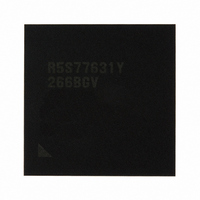
R5S77631Y266BGV Renesas Electronics America, R5S77631Y266BGV Datasheet - Page 255

R5S77631Y266BGV
Manufacturer Part Number
R5S77631Y266BGV
Description
IC SUPERH MPU ROMLESS 499BGA
Manufacturer
Renesas Electronics America
Series
SuperH® SH7780r
Datasheet
1.R5S77631Y266BGV.pdf
(2056 pages)
Specifications of R5S77631Y266BGV
Core Processor
SH-4A
Core Size
32-Bit
Speed
266MHz
Connectivity
Audio Codec, I²C, MMC, SCI, SIM, SIO, SSI, USB
Peripherals
DMA, LCD, POR, WDT
Number Of I /o
107
Program Memory Type
ROMless
Ram Size
16K x 8
Voltage - Supply (vcc/vdd)
1.15 V ~ 1.35 V
Data Converters
A/D 4x10b; D/A 2x8b
Oscillator Type
External
Operating Temperature
-20°C ~ 75°C
Package / Case
499-BGA
Lead Free Status / RoHS Status
Lead free / RoHS Compliant
Eeprom Size
-
Program Memory Size
-
Available stocks
Company
Part Number
Manufacturer
Quantity
Price
Company:
Part Number:
R5S77631Y266BGV
Manufacturer:
Renesas Electronics America
Quantity:
10 000
- Current page: 255 of 2056
- Download datasheet (10Mb)
• UB: Buffered write bit
In a memory-mapped TLB access, the UB bit can be read from or written to by bit 9 in the data
array.
PTEL: The same UB bit as that in the PMB is added in bit 9 in PTEL. This UB bit is written to
the UB bit in the UTLB by the LDTLB instruction. The PPN field is extended to bits 31 to 10.
CCR.CB: The CB bit in CCR is invalid. Whether a cacheable write for the P1 area is performed
in copy-back mode or write-though mode is determined by the WT bit in the PMB.
IRMCR.MT: The MT bit in IRMCR is valid for a memory-mapped PMB write.
QACR0, QACR1: AREA0[4:2]/AREA1[4:2] fields of QACR0/QACR1 are extended to
AREA0[7:2]/AREA1[7:2] corresponding to physical address [31:26]. See section 7.2.2, Queue
Address Control Register 0 (QACR0) and section 7.2.3, Queue Address Control Register 1
(QACR1).
LSA0, LSA1, LDA0, LDA1: L0SADR, L1SADR, L0DADR and L1DADR fields are extended to
bits 31 to 10. See section 8.2.2, L Memory Transfer Source Address Register 0 (LSA0), section
8.2.3, L Memory Transfer Source Address Register 1 (LSA1), section 8.2.4, L Memory Transfer
Destination Address Register 0 (LDA0), and section 8.2.5, L Memory Transfer Destination
Address Register 1 (LDA1).
When using 32-bit address mode, the following notes should be applied to software.
1. For the SE bit switching, only switching from 0 to 1 is supported in Cache and MMU disabled
2. After switching the SE bit, an area in which the program is allocated becomes the target of the
3. When an external memory access occurs by an operand memory access located before the
4. Note that the V bit is mapped to both address array and data array in PMB registration. That is,
Specifies whether a buffered write is performed.
0: Buffered write (Subsequent processing proceeds without waiting for the write to complete.)
1: Unbuffered write (Subsequent processing is stalled until the write has completed.)
boot routine after a power-on reset or manual reset.
PMB address translation. Therefore, the area should be recorded in the PMB before switching
the SE bit. An address which may be accessed in the P1 or P2 area such as the exception
handler should also be recorded in the PMB.
MOV.L instruction which switches the SE bit, external memory space addresses accessed in
both address modes should be the same.
first write 0 to the V bit in one of arrays and then write 1 to the V bit in another array.
Section 6 Memory Management Unit (MMU)
Rev. 2.00 May 22, 2009 Page 185 of 1982
REJ09B0256-0200
Related parts for R5S77631Y266BGV
Image
Part Number
Description
Manufacturer
Datasheet
Request
R

Part Number:
Description:
KIT STARTER FOR M16C/29
Manufacturer:
Renesas Electronics America
Datasheet:

Part Number:
Description:
KIT STARTER FOR R8C/2D
Manufacturer:
Renesas Electronics America
Datasheet:

Part Number:
Description:
R0K33062P STARTER KIT
Manufacturer:
Renesas Electronics America
Datasheet:

Part Number:
Description:
KIT STARTER FOR R8C/23 E8A
Manufacturer:
Renesas Electronics America
Datasheet:

Part Number:
Description:
KIT STARTER FOR R8C/25
Manufacturer:
Renesas Electronics America
Datasheet:

Part Number:
Description:
KIT STARTER H8S2456 SHARPE DSPLY
Manufacturer:
Renesas Electronics America
Datasheet:

Part Number:
Description:
KIT STARTER FOR R8C38C
Manufacturer:
Renesas Electronics America
Datasheet:

Part Number:
Description:
KIT STARTER FOR R8C35C
Manufacturer:
Renesas Electronics America
Datasheet:

Part Number:
Description:
KIT STARTER FOR R8CL3AC+LCD APPS
Manufacturer:
Renesas Electronics America
Datasheet:

Part Number:
Description:
KIT STARTER FOR RX610
Manufacturer:
Renesas Electronics America
Datasheet:

Part Number:
Description:
KIT STARTER FOR R32C/118
Manufacturer:
Renesas Electronics America
Datasheet:

Part Number:
Description:
KIT DEV RSK-R8C/26-29
Manufacturer:
Renesas Electronics America
Datasheet:

Part Number:
Description:
KIT STARTER FOR SH7124
Manufacturer:
Renesas Electronics America
Datasheet:

Part Number:
Description:
KIT STARTER FOR H8SX/1622
Manufacturer:
Renesas Electronics America
Datasheet:

Part Number:
Description:
KIT DEV FOR SH7203
Manufacturer:
Renesas Electronics America
Datasheet:


