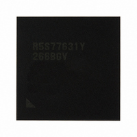
R5S77631Y266BGV Renesas Electronics America, R5S77631Y266BGV Datasheet - Page 46

R5S77631Y266BGV
Manufacturer Part Number
R5S77631Y266BGV
Description
IC SUPERH MPU ROMLESS 499BGA
Manufacturer
Renesas Electronics America
Series
SuperH® SH7780r
Datasheet
1.R5S77631Y266BGV.pdf
(2056 pages)
Specifications of R5S77631Y266BGV
Core Processor
SH-4A
Core Size
32-Bit
Speed
266MHz
Connectivity
Audio Codec, I²C, MMC, SCI, SIM, SIO, SSI, USB
Peripherals
DMA, LCD, POR, WDT
Number Of I /o
107
Program Memory Type
ROMless
Ram Size
16K x 8
Voltage - Supply (vcc/vdd)
1.15 V ~ 1.35 V
Data Converters
A/D 4x10b; D/A 2x8b
Oscillator Type
External
Operating Temperature
-20°C ~ 75°C
Package / Case
499-BGA
Lead Free Status / RoHS Status
Lead free / RoHS Compliant
Eeprom Size
-
Program Memory Size
-
Available stocks
Company
Part Number
Manufacturer
Quantity
Price
Company:
Part Number:
R5S77631Y266BGV
Manufacturer:
Renesas Electronics America
Quantity:
10 000
- Current page: 46 of 2056
- Download datasheet (10Mb)
Figure 14.11 DMA Transfer Flowchart...................................................................................... 609
Figure 14.12 Reload Mode Transfer........................................................................................... 611
Figure 14.13 Example of DREQ Input Detection in Cycle Steal Mode Edge Detection............ 612
Figure 14.14 Example of DREQ Input Detection in Cycle Steal Mode Level Detection........... 612
Figure 14.15 Example of DREQ Input Detection in Burst Mode Edge Detection ..................... 613
Figure 14.16 Example of DREQ Input Detection in Burst Mode Level Detection .................... 613
Figure 14.17 DMA Transfer End Signal (Cycle Steal Mode Level Detection) .......................... 614
Figure 14.18 Example of BSC Ordinary Memory Access
Section 15 External CPU Interface (EXCPU)
Figure 15.1 EXCPU Block Diagram .......................................................................................... 623
Figure 15.2 External CPU Access (Single Access) .................................................................... 632
Figure 15.3 External CPU Access (Burst Access)...................................................................... 633
Figure 15.4 Configuration of Connection with External CPU.................................................... 634
Section 16 Clock Pulse Generator (CPG)
Figure 16.1 Block Diagram of CPG ........................................................................................... 636
Figure 16.2 Notes on Using Crystal Resonator .......................................................................... 644
Figure 16.3 Notes on Using PLL or DLL Oscillator Circuit ...................................................... 645
Section 17 Watchdog Timer and Reset (WDT)
Figure 17.1 System Block Diagram............................................................................................ 648
Figure 17.2 WDT Counting Up Operation ................................................................................. 659
Figure 17.3 STATUS Output during Power-on.......................................................................... 662
Figure 17.4 STATUS Output by Reset input during Normal Operation .................................... 663
Figure 17.5 STATUS Output by Reset input during Sleep Mode .............................................. 663
Figure 17.6 STATUS Output by Watchdog timer overflow Power-On Reset during Normal
Figure 17.7 STATUS Output by Watchdog timer overflow Power-On Reset during Sleep
Figure 17.8 STATUS Output by Watchdog timer overflow Manual Reset during Normal
Figure 17.9 STATUS Output by Watchdog timer overflow Manual Reset during Sleep
Section 18 Power-Down Mode
Figure 18.1 DDR-SDRAM Interface Operation when Turning System Power Supply On/
Figure 18.2 Sequence for Turning Off System Power Supply after Entering Self-Refresh
Figure 18.3 Sequence for Turning VDD Power Supply (1.2 V) On/Off .................................... 687
Rev. 2.00 May 22, 2009 Page xliv of lxviii
Off ........................................................................................................................... 684
Mode........................................................................................................................ 685
Operation................................................................................................................. 664
Mode ....................................................................................................................... 665
Operation................................................................................................................. 666
Mode ....................................................................................................................... 667
(No Wait, Idle Cycle 1, Longword Access to 16-Bit Device) ............................... 615
Related parts for R5S77631Y266BGV
Image
Part Number
Description
Manufacturer
Datasheet
Request
R

Part Number:
Description:
KIT STARTER FOR M16C/29
Manufacturer:
Renesas Electronics America
Datasheet:

Part Number:
Description:
KIT STARTER FOR R8C/2D
Manufacturer:
Renesas Electronics America
Datasheet:

Part Number:
Description:
R0K33062P STARTER KIT
Manufacturer:
Renesas Electronics America
Datasheet:

Part Number:
Description:
KIT STARTER FOR R8C/23 E8A
Manufacturer:
Renesas Electronics America
Datasheet:

Part Number:
Description:
KIT STARTER FOR R8C/25
Manufacturer:
Renesas Electronics America
Datasheet:

Part Number:
Description:
KIT STARTER H8S2456 SHARPE DSPLY
Manufacturer:
Renesas Electronics America
Datasheet:

Part Number:
Description:
KIT STARTER FOR R8C38C
Manufacturer:
Renesas Electronics America
Datasheet:

Part Number:
Description:
KIT STARTER FOR R8C35C
Manufacturer:
Renesas Electronics America
Datasheet:

Part Number:
Description:
KIT STARTER FOR R8CL3AC+LCD APPS
Manufacturer:
Renesas Electronics America
Datasheet:

Part Number:
Description:
KIT STARTER FOR RX610
Manufacturer:
Renesas Electronics America
Datasheet:

Part Number:
Description:
KIT STARTER FOR R32C/118
Manufacturer:
Renesas Electronics America
Datasheet:

Part Number:
Description:
KIT DEV RSK-R8C/26-29
Manufacturer:
Renesas Electronics America
Datasheet:

Part Number:
Description:
KIT STARTER FOR SH7124
Manufacturer:
Renesas Electronics America
Datasheet:

Part Number:
Description:
KIT STARTER FOR H8SX/1622
Manufacturer:
Renesas Electronics America
Datasheet:

Part Number:
Description:
KIT DEV FOR SH7203
Manufacturer:
Renesas Electronics America
Datasheet:


