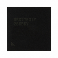
R5S77631Y266BGV Renesas Electronics America, R5S77631Y266BGV Datasheet - Page 1157

R5S77631Y266BGV
Manufacturer Part Number
R5S77631Y266BGV
Description
IC SUPERH MPU ROMLESS 499BGA
Manufacturer
Renesas Electronics America
Series
SuperH® SH7780r
Datasheet
1.R5S77631Y266BGV.pdf
(2056 pages)
Specifications of R5S77631Y266BGV
Core Processor
SH-4A
Core Size
32-Bit
Speed
266MHz
Connectivity
Audio Codec, I²C, MMC, SCI, SIM, SIO, SSI, USB
Peripherals
DMA, LCD, POR, WDT
Number Of I /o
107
Program Memory Type
ROMless
Ram Size
16K x 8
Voltage - Supply (vcc/vdd)
1.15 V ~ 1.35 V
Data Converters
A/D 4x10b; D/A 2x8b
Oscillator Type
External
Operating Temperature
-20°C ~ 75°C
Package / Case
499-BGA
Lead Free Status / RoHS Status
Lead free / RoHS Compliant
Eeprom Size
-
Program Memory Size
-
Available stocks
Company
Part Number
Manufacturer
Quantity
Price
Company:
Part Number:
R5S77631Y266BGV
Manufacturer:
Renesas Electronics America
Quantity:
10 000
- Current page: 1157 of 2056
- Download datasheet (10Mb)
Notes: 1. Figures in parentheses are the number of empty bytes in SCFTDR when the flag is set.
Bit
5
4
3
2
1
0
2. SCIF_CTS is fixed at active-0 regardless of the input value, and SCIF_RTS output is
3. A reset operation is performed in the event of a power-on reset or manual reset.
Bit Name
TTRG1
TTRG0
MCE
TFCL
RFCL
LOOP
also fixed at 0.
Initial
Value
0
0
0
0
0
0
R/W
R/W
R/W
R/W
R/W
R/W
R/W
Description
Transmit FIFO Data Number Trigger
These bits are used to set the number of remaining
transmit data bytes that sets the TDFE flag in SCFSR.
The TDFE flag is set when the number of transmit data
bytes in SCFTDR is equal to or less than the trigger set
number shown below.
00: 32 (32)
01:16 (48)
10: 2 (62)
11: 0 (64)
Modem Control Enable
Enables the SCIF_CTS and SCIF_RTS modem control
signals. Always set the MCE bit to 0 in clocked
synchronous mode.
0: Modem signals disabled*
1: Modem signals enabled
Transmit FIFO Data Register Reset
Invalidates the transmit data in the transmit FIFO data
register and resets it to the empty state.
0: Reset operation disabled*
1: Reset operation enabled
Receive FIFO Data Register Reset
Invalidates the receive data in the receive FIFO data
register and resets it to the empty state.
0: Reset operation disabled*
1: Reset operation enabled
Loopback Test
Internally connects the transmit output pin (SCIF_TXD)
and receive input pin (SCIF_RXD), and the SCIF_RTS
pin and SCIF_CTS pin, enabling loopback testing.
0: Loopback test disabled
1: Loopback test enabled
Section 27 Serial Communication Interface with FIFO (SCIF)
*
1
Rev. 2.00 May 22, 2009 Page 1087 of 1982
2
3
3
REJ09B0256-0200
Related parts for R5S77631Y266BGV
Image
Part Number
Description
Manufacturer
Datasheet
Request
R

Part Number:
Description:
KIT STARTER FOR M16C/29
Manufacturer:
Renesas Electronics America
Datasheet:

Part Number:
Description:
KIT STARTER FOR R8C/2D
Manufacturer:
Renesas Electronics America
Datasheet:

Part Number:
Description:
R0K33062P STARTER KIT
Manufacturer:
Renesas Electronics America
Datasheet:

Part Number:
Description:
KIT STARTER FOR R8C/23 E8A
Manufacturer:
Renesas Electronics America
Datasheet:

Part Number:
Description:
KIT STARTER FOR R8C/25
Manufacturer:
Renesas Electronics America
Datasheet:

Part Number:
Description:
KIT STARTER H8S2456 SHARPE DSPLY
Manufacturer:
Renesas Electronics America
Datasheet:

Part Number:
Description:
KIT STARTER FOR R8C38C
Manufacturer:
Renesas Electronics America
Datasheet:

Part Number:
Description:
KIT STARTER FOR R8C35C
Manufacturer:
Renesas Electronics America
Datasheet:

Part Number:
Description:
KIT STARTER FOR R8CL3AC+LCD APPS
Manufacturer:
Renesas Electronics America
Datasheet:

Part Number:
Description:
KIT STARTER FOR RX610
Manufacturer:
Renesas Electronics America
Datasheet:

Part Number:
Description:
KIT STARTER FOR R32C/118
Manufacturer:
Renesas Electronics America
Datasheet:

Part Number:
Description:
KIT DEV RSK-R8C/26-29
Manufacturer:
Renesas Electronics America
Datasheet:

Part Number:
Description:
KIT STARTER FOR SH7124
Manufacturer:
Renesas Electronics America
Datasheet:

Part Number:
Description:
KIT STARTER FOR H8SX/1622
Manufacturer:
Renesas Electronics America
Datasheet:

Part Number:
Description:
KIT DEV FOR SH7203
Manufacturer:
Renesas Electronics America
Datasheet:


