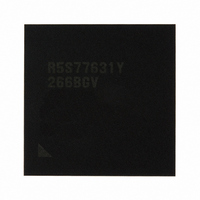
R5S77631Y266BGV Renesas Electronics America, R5S77631Y266BGV Datasheet - Page 43

R5S77631Y266BGV
Manufacturer Part Number
R5S77631Y266BGV
Description
IC SUPERH MPU ROMLESS 499BGA
Manufacturer
Renesas Electronics America
Series
SuperH® SH7780r
Datasheet
1.R5S77631Y266BGV.pdf
(2056 pages)
Specifications of R5S77631Y266BGV
Core Processor
SH-4A
Core Size
32-Bit
Speed
266MHz
Connectivity
Audio Codec, I²C, MMC, SCI, SIM, SIO, SSI, USB
Peripherals
DMA, LCD, POR, WDT
Number Of I /o
107
Program Memory Type
ROMless
Ram Size
16K x 8
Voltage - Supply (vcc/vdd)
1.15 V ~ 1.35 V
Data Converters
A/D 4x10b; D/A 2x8b
Oscillator Type
External
Operating Temperature
-20°C ~ 75°C
Package / Case
499-BGA
Lead Free Status / RoHS Status
Lead free / RoHS Compliant
Eeprom Size
-
Program Memory Size
-
Available stocks
Company
Part Number
Manufacturer
Quantity
Price
Company:
Part Number:
R5S77631Y266BGV
Manufacturer:
Renesas Electronics America
Quantity:
10 000
- Current page: 43 of 2056
- Download datasheet (10Mb)
Figure 11.7 Example of 16-Bit Data-Width SRAM Connection ................................................ 369
Figure 11.8 Example of 8-Bit Data-Width SRAM Connection .................................................. 369
Figure 11.9 SRAM Interface Wait Timing (Software Wait Only) ............................................. 370
Figure 11.10 SRAM Interface Wait Cycle Timing (Wait Cycle Insertion by RDY Signal)....... 371
Figure 11.11 SRAM Interface Wait State Timing (Read-Strobe Negate Timing Setting).......... 373
Figure 11.12 Burst ROM Basic Access Timing ......................................................................... 375
Figure 11.13 Burst ROM Wait Access Timing........................................................................... 375
Figure 11.14 Burst ROM Wait Access Timing........................................................................... 376
Figure 11.15 CExx and DACK Output of ATA Complete Mode in DMA Transfer.................. 378
Figure 11.16 Example of PCMCIA Interface ............................................................................. 381
Figure 11.17 Basic Timing for PCMCIA Memory Card Interface ............................................. 382
Figure 11.18 Wait Timing for PCMCIA Memory Card Interface .............................................. 383
Figure 11.19 Basic Timing for PCMCIA I/O Card Interface ..................................................... 384
Figure 11.20 Wait Timing for PCMCIA I/O Card Interface ...................................................... 385
Figure 11.21 Dynamic Bus Sizing Timing for PCMCIA I/O Card Interface ............................. 386
Figure 11.22 Example of 32-Bit Data Width MPX Connection ................................................. 388
Figure 11.23 MPX Interface Timing 1 (Single Read Cycle, IW = 0, No External Wait) ........... 388
Figure 11.24 MPX Interface Timing 2 (Single Read, IW = 0, One External Wait Inserted)...... 389
Figure 11.25 MPX Interface Timing 3 (Single Write Cycle, IW = 0, No External Wait) .......... 390
Figure 11.26 MPX Interface Timing 4
Figure 11.27 MPX Interface Timing 5 (Burst Read Cycle, IW = 0, No External Wait)............. 392
Figure 11.28 MPX Interface Timing 6 (Burst Read Cycle, IW = 0, External Wait Control) ..... 393
Figure 11.29 MPX Interface Timing 7 (Burst Write Cycle, IW = 0, No External Wait)............ 394
Figure 11.30 MPX Interface Timing 8 (Burst Write Cycle, IW = 1, External Wait Control) .... 395
Figure 11.31 MPX Interface Timing 9
Figure 11.32 MPX Interface Timing 10
Figure 11.33 MPX Interface Timing 11
Figure 11.34 MPX Interface Timing 12
Figure 11.35 Example of 32-Bit Data-Width Byte-Control SRAM ........................................... 400
Figure 11.36 Byte-Control SRAM Basic Read Cycle (No Wait) ............................................... 401
Figure 11.37 Byte-Control SRAM Basic Read Cycle (One Internal Wait Cycle)...................... 402
(Single Write Cycle, IW = 1, One External Wait Inserted) .................................. 391
(Burst Read Cycle, IW = 0, No External Wait, 32-Bit Bus Width,
32-Byte Data Transfer) .......................................................................................... 396
(Burst Read Cycle, IW = 0, External Wait Control, 32-Bit Bus Width,
32-Byte Data Transfer) .......................................................................................... 397
(Burst Write Cycle, IW = 0, No External Wait, 32-Bit Bus Width,
32-Byte Data Transfer) .......................................................................................... 398
(Burst Write Cycle, IW = 1, External Wait Control, 32-Bit Bus Width,
32-Byte Data Transfer) .......................................................................................... 399
Rev. 2.00 May 22, 2009 Page xli of lxviii
Related parts for R5S77631Y266BGV
Image
Part Number
Description
Manufacturer
Datasheet
Request
R

Part Number:
Description:
KIT STARTER FOR M16C/29
Manufacturer:
Renesas Electronics America
Datasheet:

Part Number:
Description:
KIT STARTER FOR R8C/2D
Manufacturer:
Renesas Electronics America
Datasheet:

Part Number:
Description:
R0K33062P STARTER KIT
Manufacturer:
Renesas Electronics America
Datasheet:

Part Number:
Description:
KIT STARTER FOR R8C/23 E8A
Manufacturer:
Renesas Electronics America
Datasheet:

Part Number:
Description:
KIT STARTER FOR R8C/25
Manufacturer:
Renesas Electronics America
Datasheet:

Part Number:
Description:
KIT STARTER H8S2456 SHARPE DSPLY
Manufacturer:
Renesas Electronics America
Datasheet:

Part Number:
Description:
KIT STARTER FOR R8C38C
Manufacturer:
Renesas Electronics America
Datasheet:

Part Number:
Description:
KIT STARTER FOR R8C35C
Manufacturer:
Renesas Electronics America
Datasheet:

Part Number:
Description:
KIT STARTER FOR R8CL3AC+LCD APPS
Manufacturer:
Renesas Electronics America
Datasheet:

Part Number:
Description:
KIT STARTER FOR RX610
Manufacturer:
Renesas Electronics America
Datasheet:

Part Number:
Description:
KIT STARTER FOR R32C/118
Manufacturer:
Renesas Electronics America
Datasheet:

Part Number:
Description:
KIT DEV RSK-R8C/26-29
Manufacturer:
Renesas Electronics America
Datasheet:

Part Number:
Description:
KIT STARTER FOR SH7124
Manufacturer:
Renesas Electronics America
Datasheet:

Part Number:
Description:
KIT STARTER FOR H8SX/1622
Manufacturer:
Renesas Electronics America
Datasheet:

Part Number:
Description:
KIT DEV FOR SH7203
Manufacturer:
Renesas Electronics America
Datasheet:


