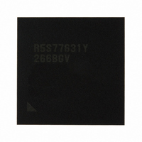
R5S77631Y266BGV Renesas Electronics America, R5S77631Y266BGV Datasheet - Page 261

R5S77631Y266BGV
Manufacturer Part Number
R5S77631Y266BGV
Description
IC SUPERH MPU ROMLESS 499BGA
Manufacturer
Renesas Electronics America
Series
SuperH® SH7780r
Datasheet
1.R5S77631Y266BGV.pdf
(2056 pages)
Specifications of R5S77631Y266BGV
Core Processor
SH-4A
Core Size
32-Bit
Speed
266MHz
Connectivity
Audio Codec, I²C, MMC, SCI, SIM, SIO, SSI, USB
Peripherals
DMA, LCD, POR, WDT
Number Of I /o
107
Program Memory Type
ROMless
Ram Size
16K x 8
Voltage - Supply (vcc/vdd)
1.15 V ~ 1.35 V
Data Converters
A/D 4x10b; D/A 2x8b
Oscillator Type
External
Operating Temperature
-20°C ~ 75°C
Package / Case
499-BGA
Lead Free Status / RoHS Status
Lead free / RoHS Compliant
Eeprom Size
-
Program Memory Size
-
Available stocks
Company
Part Number
Manufacturer
Quantity
Price
Company:
Part Number:
R5S77631Y266BGV
Manufacturer:
Renesas Electronics America
Quantity:
10 000
- Current page: 261 of 2056
- Download datasheet (10Mb)
7.2.1
CCR controls the cache operating mode, the cache write mode, and invalidation of all cache
entries.
CCR modifications must only be made by a program in the non-cacheable P2 area. After CCR has
been updated, execute one of the following three methods before an access (including an
instruction fetch) to the cacheable area is performed.
1. Execute a branch using the RTE instruction. In this case, the branch destination may be the
2. Execute the ICBI instruction for any address (including non-cacheable area).
3. If the R2 bit in IRMCR is 0 (initial value) before updating CCR, the specific instruction does
Note that the method 3 may not be guaranteed in the future SuperH Series. Therefore, it is
recommended that the method 1 or 2 should be used for being compatible with the future SuperH
Series.
Initial value:
Initial value:
Bit
31 to 12
11
cacheable area.
not need to be executed. However, note that the CPU processing performance will be lowered
because the instruction fetch is performed again for the next instruction after CCR has been
updated.
R/W:
R/W:
Bit:
Bit:
Cache Control Register (CCR)
Bit Name
ICI
31
15
R
R
0
0
30
14
R
R
0
0
29
13
R
R
0
0
Initial
Value
All 0
0
28
12
R
R
0
0
R/W
ICI
27
11
R
0
0
R/W
R
R/W
26
10
R
R
0
0
Description
Reserved
For details on reading from or writing to these bits, see
description in General Precautions on Handling of
Product.
IC Invalidation Bit
When 1 is written to this bit, the V bits of all IC entries
are cleared to 0. This bit is always read as 0.
25
R
R
0
9
0
R/W
ICE
24
R
0
8
0
23
R
R
0
7
0
Rev. 2.00 May 22, 2009 Page 191 of 1982
22
R
R
0
6
0
21
R
R
0
5
0
20
R
R
0
4
0
R/W
OCI
19
R
0
3
0
Section 7 Caches
REJ09B0256-0200
R/W
CB
18
R
2
0
0
R/W
WT
17
R
0
1
0
OCE
R/W
16
R
0
0
0
Related parts for R5S77631Y266BGV
Image
Part Number
Description
Manufacturer
Datasheet
Request
R

Part Number:
Description:
KIT STARTER FOR M16C/29
Manufacturer:
Renesas Electronics America
Datasheet:

Part Number:
Description:
KIT STARTER FOR R8C/2D
Manufacturer:
Renesas Electronics America
Datasheet:

Part Number:
Description:
R0K33062P STARTER KIT
Manufacturer:
Renesas Electronics America
Datasheet:

Part Number:
Description:
KIT STARTER FOR R8C/23 E8A
Manufacturer:
Renesas Electronics America
Datasheet:

Part Number:
Description:
KIT STARTER FOR R8C/25
Manufacturer:
Renesas Electronics America
Datasheet:

Part Number:
Description:
KIT STARTER H8S2456 SHARPE DSPLY
Manufacturer:
Renesas Electronics America
Datasheet:

Part Number:
Description:
KIT STARTER FOR R8C38C
Manufacturer:
Renesas Electronics America
Datasheet:

Part Number:
Description:
KIT STARTER FOR R8C35C
Manufacturer:
Renesas Electronics America
Datasheet:

Part Number:
Description:
KIT STARTER FOR R8CL3AC+LCD APPS
Manufacturer:
Renesas Electronics America
Datasheet:

Part Number:
Description:
KIT STARTER FOR RX610
Manufacturer:
Renesas Electronics America
Datasheet:

Part Number:
Description:
KIT STARTER FOR R32C/118
Manufacturer:
Renesas Electronics America
Datasheet:

Part Number:
Description:
KIT DEV RSK-R8C/26-29
Manufacturer:
Renesas Electronics America
Datasheet:

Part Number:
Description:
KIT STARTER FOR SH7124
Manufacturer:
Renesas Electronics America
Datasheet:

Part Number:
Description:
KIT STARTER FOR H8SX/1622
Manufacturer:
Renesas Electronics America
Datasheet:

Part Number:
Description:
KIT DEV FOR SH7203
Manufacturer:
Renesas Electronics America
Datasheet:


