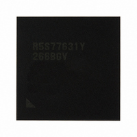
R5S77631Y266BGV Renesas Electronics America, R5S77631Y266BGV Datasheet - Page 1266

R5S77631Y266BGV
Manufacturer Part Number
R5S77631Y266BGV
Description
IC SUPERH MPU ROMLESS 499BGA
Manufacturer
Renesas Electronics America
Series
SuperH® SH7780r
Datasheet
1.R5S77631Y266BGV.pdf
(2056 pages)
Specifications of R5S77631Y266BGV
Core Processor
SH-4A
Core Size
32-Bit
Speed
266MHz
Connectivity
Audio Codec, I²C, MMC, SCI, SIM, SIO, SSI, USB
Peripherals
DMA, LCD, POR, WDT
Number Of I /o
107
Program Memory Type
ROMless
Ram Size
16K x 8
Voltage - Supply (vcc/vdd)
1.15 V ~ 1.35 V
Data Converters
A/D 4x10b; D/A 2x8b
Oscillator Type
External
Operating Temperature
-20°C ~ 75°C
Package / Case
499-BGA
Lead Free Status / RoHS Status
Lead free / RoHS Compliant
Eeprom Size
-
Program Memory Size
-
Available stocks
Company
Part Number
Manufacturer
Quantity
Price
Company:
Part Number:
R5S77631Y266BGV
Manufacturer:
Renesas Electronics America
Quantity:
10 000
- Current page: 1266 of 2056
- Download datasheet (10Mb)
Section 29 Serial I/O with FIFO (SIOF)
Table 29.4 shows the operation in each transfer mode.
Table 29.4 Operation in Each Transfer Mode
Note:
29.3.2
SISCR is a 16-bit readable/writable register that sets the serial clock generation conditions for the
master clock. SISCR can be specified when the bits TRMD[1:0] in SIMDR are specified as B'10
or B'11.
Rev. 2.00 May 22, 2009 Page 1196 of 1982
REJ09B0256-0200
Initial value:
Transfer Mode
Slave mode 1
Slave mode 2
Master mode 1
Master mode 2
Bit
15
14
13
R/W:
BIt:
*
Clock Select Register (SISCR)
Bit Name
MSSEL
MSIMM
—
MSSEL MSIMM
The control data method is valid only when the FL bit is specified as B'1xxx. (x: don't
care.)
R/W
15
1
R/W
14
1
Master
Master
Master/Slave
Slave
Slave
13
—
R
0
Initial
Value
1
1
0
R/W
12
0
R/W
R/W
R/W
R
R/W
11
0
SIOF_SYNC
Synchronous pulse
Synchronous pulse
Synchronous pulse
L/R
BRPS[4:0]
R/W
10
0
Description
Master Clock Source Selection
The master clock is the clock source input to the baud
rate generator (prescaler).
0: Uses the input clock signal of the SIOF_MCLK pin as
1: Uses Pck0 as the master clock
Master Clock Direct Selection
0: Uses the output clock of the baud rate generator as
1: Uses the master clock itself as the serial clock
Reserved
This bit is always read as 0. The write value should
always be 0.
R/W
the master clock
the serial clock
9
0
R/W
8
0
—
R
7
0
Bit Delay
SYNCDL bit
No
—
R
6
0
—
R
5
0
—
Control Data Method*
Slot position
Secondary FS
Slot position
Not supported
R
4
0
—
R
3
0
R/W
2
0
BRDV[2:0]
R/W
1
0
R/W
0
0
Related parts for R5S77631Y266BGV
Image
Part Number
Description
Manufacturer
Datasheet
Request
R

Part Number:
Description:
KIT STARTER FOR M16C/29
Manufacturer:
Renesas Electronics America
Datasheet:

Part Number:
Description:
KIT STARTER FOR R8C/2D
Manufacturer:
Renesas Electronics America
Datasheet:

Part Number:
Description:
R0K33062P STARTER KIT
Manufacturer:
Renesas Electronics America
Datasheet:

Part Number:
Description:
KIT STARTER FOR R8C/23 E8A
Manufacturer:
Renesas Electronics America
Datasheet:

Part Number:
Description:
KIT STARTER FOR R8C/25
Manufacturer:
Renesas Electronics America
Datasheet:

Part Number:
Description:
KIT STARTER H8S2456 SHARPE DSPLY
Manufacturer:
Renesas Electronics America
Datasheet:

Part Number:
Description:
KIT STARTER FOR R8C38C
Manufacturer:
Renesas Electronics America
Datasheet:

Part Number:
Description:
KIT STARTER FOR R8C35C
Manufacturer:
Renesas Electronics America
Datasheet:

Part Number:
Description:
KIT STARTER FOR R8CL3AC+LCD APPS
Manufacturer:
Renesas Electronics America
Datasheet:

Part Number:
Description:
KIT STARTER FOR RX610
Manufacturer:
Renesas Electronics America
Datasheet:

Part Number:
Description:
KIT STARTER FOR R32C/118
Manufacturer:
Renesas Electronics America
Datasheet:

Part Number:
Description:
KIT DEV RSK-R8C/26-29
Manufacturer:
Renesas Electronics America
Datasheet:

Part Number:
Description:
KIT STARTER FOR SH7124
Manufacturer:
Renesas Electronics America
Datasheet:

Part Number:
Description:
KIT STARTER FOR H8SX/1622
Manufacturer:
Renesas Electronics America
Datasheet:

Part Number:
Description:
KIT DEV FOR SH7203
Manufacturer:
Renesas Electronics America
Datasheet:


