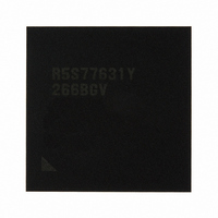
R5S77631Y266BGV Renesas Electronics America, R5S77631Y266BGV Datasheet - Page 57

R5S77631Y266BGV
Manufacturer Part Number
R5S77631Y266BGV
Description
IC SUPERH MPU ROMLESS 499BGA
Manufacturer
Renesas Electronics America
Series
SuperH® SH7780r
Datasheet
1.R5S77631Y266BGV.pdf
(2056 pages)
Specifications of R5S77631Y266BGV
Core Processor
SH-4A
Core Size
32-Bit
Speed
266MHz
Connectivity
Audio Codec, I²C, MMC, SCI, SIM, SIO, SSI, USB
Peripherals
DMA, LCD, POR, WDT
Number Of I /o
107
Program Memory Type
ROMless
Ram Size
16K x 8
Voltage - Supply (vcc/vdd)
1.15 V ~ 1.35 V
Data Converters
A/D 4x10b; D/A 2x8b
Oscillator Type
External
Operating Temperature
-20°C ~ 75°C
Package / Case
499-BGA
Lead Free Status / RoHS Status
Lead free / RoHS Compliant
Eeprom Size
-
Program Memory Size
-
Available stocks
Company
Part Number
Manufacturer
Quantity
Price
Company:
Part Number:
R5S77631Y266BGV
Manufacturer:
Renesas Electronics America
Quantity:
10 000
- Current page: 57 of 2056
- Download datasheet (10Mb)
Figure 43.17 Burst ROM Bus Cycle
Figure 43.18 Burst ROM Bus Cycle (One Wait by Software + One Wait by RDY)................ 1850
Figure 43.19 PCMCIA Memory Bus Cycle ............................................................................. 1851
Figure 43.20 PCMCIA I/O Bus Cycle...................................................................................... 1852
Figure 43.21 PCMCIA I/O Bus Cycle
Figure 43.22 MPX Basic Bus Cycle: Read............................................................................... 1854
Figure 43.23 MPX Basic Bus Cycle: Write.............................................................................. 1855
Figure 43.24 MPX Bus Cycle: Burst Read............................................................................... 1856
Figure 43.25 MPX Bus Cycle: Burst Write .............................................................................. 1857
Figure 43.26 Byte Control SRAM Bus Cycle .......................................................................... 1858
Figure 43.27 Byte Control SRAM Bus Cycle: Basic Read Cycle
Figure 43.28 DDRIF MCLK Output Timing............................................................................ 1861
Figure 43.29 Read Timing of DDR-SDRAM (2 Burst Read) .................................................. 1861
Figure 43.30 Write Timing of DDR-SDRAM (2 Burst Write)................................................. 1862
Figure 43.31 NMI Input Timing ............................................................................................... 1863
Figure 43.32 IRQ/IRL, PINT Input and IRQOUT Output Timing........................................... 1864
Figure 43.33 External CPU Interface Read/Write Access Timing ........................................... 1866
Figure 43.34 PCI Clock Input Timing ...................................................................................... 1868
Figure 46.35 Output Signal Timing .......................................................................................... 1868
Figure 43.36 Input Signal Timing............................................................................................. 1868
Figure 43.37 DREQ, TEND, and DACK Timing..................................................................... 1869
Figure 43.38 TCLK Input Timing ............................................................................................ 1870
Figure 43.39 TPU Output Timing............................................................................................. 1871
Figure 43.40 TPU Clock Input Timing..................................................................................... 1871
Figure 43.41 MII Transmit Timing (normal operation)............................................................ 1873
Figure 43.42 MII Receive Timing (normal operation) ............................................................. 1873
Figure 43.43 MII Receive Timing (When an Error is Detected) .............................................. 1874
Figure 43.44 WOL Output Timing ........................................................................................... 1874
Figure 43.45 GMII Transmit Timing (normal operation)......................................................... 1875
Figure 43.46 GMII Receive Timing (normal operation) .......................................................... 1875
Figure 43.47 GMII Receive Timing (When an Error is Detected) ........................................... 1876
Figure 43.48 WOL Output Timing ........................................................................................... 1876
Figure 43.49 RMII Transmit Timing ........................................................................................ 1877
Figure 43.50 RMII Receive Timing (normal operation)........................................................... 1877
Figure 43.51 RMII Receive Timing (When an Error is Detected)............................................ 1878
Figure 43.52 STIF Clock Valid Receive Timing...................................................................... 1879
Figure 43.53 STIF Clock Valid Transmit Timing .................................................................... 1880
(No Wait, No Address Setup/Hold Time Insertion, RDS = 1, RDH = 0)............ 1849
(TEDA/TEDB = 1, TEHA/TEHB = 1, IW/PCIW = 1, Dynamic Bus Sizing)..... 1853
(No Wait, No Address Setup/Hold Time Insertion, RDS = 1, RDH = 0)............ 1859
Rev. 2.00 May 22, 2009 Page lv of lxviii
Related parts for R5S77631Y266BGV
Image
Part Number
Description
Manufacturer
Datasheet
Request
R

Part Number:
Description:
KIT STARTER FOR M16C/29
Manufacturer:
Renesas Electronics America
Datasheet:

Part Number:
Description:
KIT STARTER FOR R8C/2D
Manufacturer:
Renesas Electronics America
Datasheet:

Part Number:
Description:
R0K33062P STARTER KIT
Manufacturer:
Renesas Electronics America
Datasheet:

Part Number:
Description:
KIT STARTER FOR R8C/23 E8A
Manufacturer:
Renesas Electronics America
Datasheet:

Part Number:
Description:
KIT STARTER FOR R8C/25
Manufacturer:
Renesas Electronics America
Datasheet:

Part Number:
Description:
KIT STARTER H8S2456 SHARPE DSPLY
Manufacturer:
Renesas Electronics America
Datasheet:

Part Number:
Description:
KIT STARTER FOR R8C38C
Manufacturer:
Renesas Electronics America
Datasheet:

Part Number:
Description:
KIT STARTER FOR R8C35C
Manufacturer:
Renesas Electronics America
Datasheet:

Part Number:
Description:
KIT STARTER FOR R8CL3AC+LCD APPS
Manufacturer:
Renesas Electronics America
Datasheet:

Part Number:
Description:
KIT STARTER FOR RX610
Manufacturer:
Renesas Electronics America
Datasheet:

Part Number:
Description:
KIT STARTER FOR R32C/118
Manufacturer:
Renesas Electronics America
Datasheet:

Part Number:
Description:
KIT DEV RSK-R8C/26-29
Manufacturer:
Renesas Electronics America
Datasheet:

Part Number:
Description:
KIT STARTER FOR SH7124
Manufacturer:
Renesas Electronics America
Datasheet:

Part Number:
Description:
KIT STARTER FOR H8SX/1622
Manufacturer:
Renesas Electronics America
Datasheet:

Part Number:
Description:
KIT DEV FOR SH7203
Manufacturer:
Renesas Electronics America
Datasheet:


