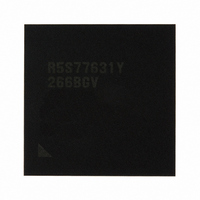
R5S77631Y266BGV Renesas Electronics America, R5S77631Y266BGV Datasheet - Page 1176

R5S77631Y266BGV
Manufacturer Part Number
R5S77631Y266BGV
Description
IC SUPERH MPU ROMLESS 499BGA
Manufacturer
Renesas Electronics America
Series
SuperH® SH7780r
Datasheet
1.R5S77631Y266BGV.pdf
(2056 pages)
Specifications of R5S77631Y266BGV
Core Processor
SH-4A
Core Size
32-Bit
Speed
266MHz
Connectivity
Audio Codec, I²C, MMC, SCI, SIM, SIO, SSI, USB
Peripherals
DMA, LCD, POR, WDT
Number Of I /o
107
Program Memory Type
ROMless
Ram Size
16K x 8
Voltage - Supply (vcc/vdd)
1.15 V ~ 1.35 V
Data Converters
A/D 4x10b; D/A 2x8b
Oscillator Type
External
Operating Temperature
-20°C ~ 75°C
Package / Case
499-BGA
Lead Free Status / RoHS Status
Lead free / RoHS Compliant
Eeprom Size
-
Program Memory Size
-
Available stocks
Company
Part Number
Manufacturer
Quantity
Price
Company:
Part Number:
R5S77631Y266BGV
Manufacturer:
Renesas Electronics America
Quantity:
10 000
- Current page: 1176 of 2056
- Download datasheet (10Mb)
Section 27 Serial Communication Interface with FIFO (SCIF)
5. When modem control is enabled, the SCIF_RTS signal is output when SCFRDR is empty.
Figure 27.14 shows an example of the operation when modem control is used.
27.4.3
Clocked synchronous mode, in which data is transmitted or received in synchronization with clock
pulses, is suitable for fast serial communication.
Since the transmitter and receiver are independent units in the SCIF, full-duplex communication
can be achieved by sharing the clock. Both the transmitter and receiver have a 64-stage FIFO
buffer structure, so that data can be read or written during transmission or reception, enabling
continuous data transfer and reception.
Figure 27.15 shows the general format for clocked synchronous communication.
Rev. 2.00 May 22, 2009 Page 1106 of 1982
REJ09B0256-0200
When SCIF0_RTS is 0, reception is possible. When SCIF_RTS is 1, this indicates that
SCFRDR contains bytes of data equal to or more than the SCIF_RTS output active trigger
number. The SCIF_RTS output active trigger value is specified by bits 10 to 8 in the FIFO
control register (SCFCR). For details, see section 27.3.9, FIFO control register (SCFCR). In
addition, SCIF_RTS is also 1 when the RE bit in SCSCR is cleared to 0.
SCIF_RXD
SCIF_RTS
Serial data
Synchronization
clock
Serial data
Note: * High except in continuous transfer
Operation in Clocked Synchronous Mode
Figure 27.14 Sample Operation Using Modem Control (SCIF0_RTS)
Figure 27.15 Data Format in Clocked Synchronous Communication
Start
bit
0
Don't care
D0
*
D1 D2
LSB
Bit 0
Bit 1
(Only in Channel 0)
One unit of transfer data (character or frame)
D7 0/1 1
Parity
bit
Bit 2
Stop
bit
Bit 3
Bit 4
Bit 5
Start
bit
0
Bit 6
Bit 7
MSB
Don't care
*
Related parts for R5S77631Y266BGV
Image
Part Number
Description
Manufacturer
Datasheet
Request
R

Part Number:
Description:
KIT STARTER FOR M16C/29
Manufacturer:
Renesas Electronics America
Datasheet:

Part Number:
Description:
KIT STARTER FOR R8C/2D
Manufacturer:
Renesas Electronics America
Datasheet:

Part Number:
Description:
R0K33062P STARTER KIT
Manufacturer:
Renesas Electronics America
Datasheet:

Part Number:
Description:
KIT STARTER FOR R8C/23 E8A
Manufacturer:
Renesas Electronics America
Datasheet:

Part Number:
Description:
KIT STARTER FOR R8C/25
Manufacturer:
Renesas Electronics America
Datasheet:

Part Number:
Description:
KIT STARTER H8S2456 SHARPE DSPLY
Manufacturer:
Renesas Electronics America
Datasheet:

Part Number:
Description:
KIT STARTER FOR R8C38C
Manufacturer:
Renesas Electronics America
Datasheet:

Part Number:
Description:
KIT STARTER FOR R8C35C
Manufacturer:
Renesas Electronics America
Datasheet:

Part Number:
Description:
KIT STARTER FOR R8CL3AC+LCD APPS
Manufacturer:
Renesas Electronics America
Datasheet:

Part Number:
Description:
KIT STARTER FOR RX610
Manufacturer:
Renesas Electronics America
Datasheet:

Part Number:
Description:
KIT STARTER FOR R32C/118
Manufacturer:
Renesas Electronics America
Datasheet:

Part Number:
Description:
KIT DEV RSK-R8C/26-29
Manufacturer:
Renesas Electronics America
Datasheet:

Part Number:
Description:
KIT STARTER FOR SH7124
Manufacturer:
Renesas Electronics America
Datasheet:

Part Number:
Description:
KIT STARTER FOR H8SX/1622
Manufacturer:
Renesas Electronics America
Datasheet:

Part Number:
Description:
KIT DEV FOR SH7203
Manufacturer:
Renesas Electronics America
Datasheet:


