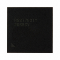
R5S77631Y266BGV Renesas Electronics America, R5S77631Y266BGV Datasheet - Page 392

R5S77631Y266BGV
Manufacturer Part Number
R5S77631Y266BGV
Description
IC SUPERH MPU ROMLESS 499BGA
Manufacturer
Renesas Electronics America
Series
SuperH® SH7780r
Datasheet
1.R5S77631Y266BGV.pdf
(2056 pages)
Specifications of R5S77631Y266BGV
Core Processor
SH-4A
Core Size
32-Bit
Speed
266MHz
Connectivity
Audio Codec, I²C, MMC, SCI, SIM, SIO, SSI, USB
Peripherals
DMA, LCD, POR, WDT
Number Of I /o
107
Program Memory Type
ROMless
Ram Size
16K x 8
Voltage - Supply (vcc/vdd)
1.15 V ~ 1.35 V
Data Converters
A/D 4x10b; D/A 2x8b
Oscillator Type
External
Operating Temperature
-20°C ~ 75°C
Package / Case
499-BGA
Lead Free Status / RoHS Status
Lead free / RoHS Compliant
Eeprom Size
-
Program Memory Size
-
Available stocks
Company
Part Number
Manufacturer
Quantity
Price
Company:
Part Number:
R5S77631Y266BGV
Manufacturer:
Renesas Electronics America
Quantity:
10 000
- Current page: 392 of 2056
- Download datasheet (10Mb)
Section 11 Local Bus State Controller (LBSC)
11.2
Table 11.1 shows the LBSC pin configuration.
Table 11.1 Pin Configuration
Rev. 2.00 May 22, 2009 Page 322 of 1982
REJ09B0256-0200
Pin Name
A25 to A0
D31 to D0
BS
CS6 to CS4,
CS2 to CS0
RDWR
RD/FRAME
WE0/PCC_REG
WE1/WE
WE2/IORD
WE3/IOWR
RDY
IOIS16
Input/Output Pins
Function
Address Bus
Data Bus
Bus Cycle Start Output
Chip Select 6 to
4 and 2 to 0
Read/Write
Read/Cycle
Frame
Data Enable 0
Data Enable 1
Data Enable 2
Data Enable 3
Ready
16-Bit I/O
Output
I/O
Output
Output
Output
Output
Output
Output
Output
Input
I/O
Input
Description
Address output
Data input/output
Signal that indicates the start of a bus cycle.
Asserted once for a burst transfer when setting
MPX interface.
Asserted each data cycle for a burst transfer
when setting other interfaces.
Chip select signal that indicates the area being
accessed. CS5 and CS6 can also be used as
CE1A to CE1B of PCMCIA.
Data bus input/output direction designation
signal. Also used as PCMCIA interface write
designation signal.
Strobe signal indicating a read cycle. FRAME
signal when setting MPX interface.
When setting SRAM interface: write strobe
signal for D7 to D0
When setting PCMCIA interface: REG signal
When setting SRAM interface: write strobe
signal for D15 to D8
When setting PCMCIA interface: Write strobe
signal
When setting SRAM interface: write strobe
signal for D23 to D16
When setting PCMCIA interface: IORD signal
When setting SRAM interface: write strobe
signal for D31 to D24
When setting PCMCIA interface: IOWR signal
Wait cycle request signal
16-bit I/O signal when setting PCMCIA interface.
Valid only in little endian mode
Related parts for R5S77631Y266BGV
Image
Part Number
Description
Manufacturer
Datasheet
Request
R

Part Number:
Description:
KIT STARTER FOR M16C/29
Manufacturer:
Renesas Electronics America
Datasheet:

Part Number:
Description:
KIT STARTER FOR R8C/2D
Manufacturer:
Renesas Electronics America
Datasheet:

Part Number:
Description:
R0K33062P STARTER KIT
Manufacturer:
Renesas Electronics America
Datasheet:

Part Number:
Description:
KIT STARTER FOR R8C/23 E8A
Manufacturer:
Renesas Electronics America
Datasheet:

Part Number:
Description:
KIT STARTER FOR R8C/25
Manufacturer:
Renesas Electronics America
Datasheet:

Part Number:
Description:
KIT STARTER H8S2456 SHARPE DSPLY
Manufacturer:
Renesas Electronics America
Datasheet:

Part Number:
Description:
KIT STARTER FOR R8C38C
Manufacturer:
Renesas Electronics America
Datasheet:

Part Number:
Description:
KIT STARTER FOR R8C35C
Manufacturer:
Renesas Electronics America
Datasheet:

Part Number:
Description:
KIT STARTER FOR R8CL3AC+LCD APPS
Manufacturer:
Renesas Electronics America
Datasheet:

Part Number:
Description:
KIT STARTER FOR RX610
Manufacturer:
Renesas Electronics America
Datasheet:

Part Number:
Description:
KIT STARTER FOR R32C/118
Manufacturer:
Renesas Electronics America
Datasheet:

Part Number:
Description:
KIT DEV RSK-R8C/26-29
Manufacturer:
Renesas Electronics America
Datasheet:

Part Number:
Description:
KIT STARTER FOR SH7124
Manufacturer:
Renesas Electronics America
Datasheet:

Part Number:
Description:
KIT STARTER FOR H8SX/1622
Manufacturer:
Renesas Electronics America
Datasheet:

Part Number:
Description:
KIT DEV FOR SH7203
Manufacturer:
Renesas Electronics America
Datasheet:


