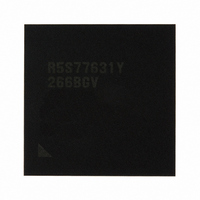
R5S77631Y266BGV Renesas Electronics America, R5S77631Y266BGV Datasheet - Page 2035

R5S77631Y266BGV
Manufacturer Part Number
R5S77631Y266BGV
Description
IC SUPERH MPU ROMLESS 499BGA
Manufacturer
Renesas Electronics America
Series
SuperH® SH7780r
Datasheet
1.R5S77631Y266BGV.pdf
(2056 pages)
Specifications of R5S77631Y266BGV
Core Processor
SH-4A
Core Size
32-Bit
Speed
266MHz
Connectivity
Audio Codec, I²C, MMC, SCI, SIM, SIO, SSI, USB
Peripherals
DMA, LCD, POR, WDT
Number Of I /o
107
Program Memory Type
ROMless
Ram Size
16K x 8
Voltage - Supply (vcc/vdd)
1.15 V ~ 1.35 V
Data Converters
A/D 4x10b; D/A 2x8b
Oscillator Type
External
Operating Temperature
-20°C ~ 75°C
Package / Case
499-BGA
Lead Free Status / RoHS Status
Lead free / RoHS Compliant
Eeprom Size
-
Program Memory Size
-
Available stocks
Company
Part Number
Manufacturer
Quantity
Price
Company:
Part Number:
R5S77631Y266BGV
Manufacturer:
Renesas Electronics America
Quantity:
10 000
- Current page: 2035 of 2056
- Download datasheet (10Mb)
Item
40.3.2 Port Input
Function
40.3.3 Peripheral
Module Function
Section 43 Electrical
Characteristics
43.2.3 Power-Off and
Power-On Order in RTC
Power-Supply Backup
Mode (Hardware
Standby)
43.2.4 Power-Off and
Power-On Order in
DDR-SDRAM Power-
Supply Backup Mode
43.2.5 Note when DDR-
SDRAM Power-Supply is
Turned On
Page
1760
1760
1830
1830
1830
Revision (See Manual for Details)
Amended
To set up a pin for the port input function (only in case of the pin
with a pull-up MOS), write B'10 (when not using MOS pull-up) or
B'11 (when using MOS pull-up) to the corresponding two bits in
the port control register (PACR to PPCR). This allows the value
of that pin to be read from the corresponding bit in the port data
register (PADR to PPDR).
Note that settings in the pull-up control register (PIPUPR to
POPUPR) and pin select register (PSEL0 to PSEL4) are invalid
for the pins configured for the port output function.
Amended
Then, if the pin is to be used as an input or input/output pin, set
the pull-up control register (PIPUPR to POPUPR) to create the
MOS pull-up setting: to the corresponding bit, write 0 when not
using the MOS pull-up or write 1 when using the MOS pull-up.
For a pin used for output, the MOS pull-up is always turned off
for any setting of the pull-up control register.
Amended
Turn on the power supplies (VCCQ, AVCC), (VCCQ-DDR), and
(VDD, VDD-PLL1 to 3, VDD-DLL1 to 3) while the XRTCSTBI pin
is low. Only after the power-on oscillation settling time (refer to
section 43.4.1, Clock and Control Signal Timing) has elapsed
after the power supplies above become stable, bring the
XRTCSTBI pin high and negate the PRESET pin to high level.
Amended
Turn on the power supplies (VCCQ, AVCC, VDD-RTC) and
(VDD, VDD-PLL1 to 3, VDD-DLL1 to 3) while the M_BKPRST
pin is low. Only after the power-on oscillation settling time (refer
to section 43.4.1, Clock and Control Signal Timing) has elapsed
after the power supplies above become stable, negate the
M_BKPRST and PRESET pins to high level.
Added
Rev. 2.00 May 22, 2009 Page 1965 of 1982
REJ09B0256-0200
Related parts for R5S77631Y266BGV
Image
Part Number
Description
Manufacturer
Datasheet
Request
R

Part Number:
Description:
KIT STARTER FOR M16C/29
Manufacturer:
Renesas Electronics America
Datasheet:

Part Number:
Description:
KIT STARTER FOR R8C/2D
Manufacturer:
Renesas Electronics America
Datasheet:

Part Number:
Description:
R0K33062P STARTER KIT
Manufacturer:
Renesas Electronics America
Datasheet:

Part Number:
Description:
KIT STARTER FOR R8C/23 E8A
Manufacturer:
Renesas Electronics America
Datasheet:

Part Number:
Description:
KIT STARTER FOR R8C/25
Manufacturer:
Renesas Electronics America
Datasheet:

Part Number:
Description:
KIT STARTER H8S2456 SHARPE DSPLY
Manufacturer:
Renesas Electronics America
Datasheet:

Part Number:
Description:
KIT STARTER FOR R8C38C
Manufacturer:
Renesas Electronics America
Datasheet:

Part Number:
Description:
KIT STARTER FOR R8C35C
Manufacturer:
Renesas Electronics America
Datasheet:

Part Number:
Description:
KIT STARTER FOR R8CL3AC+LCD APPS
Manufacturer:
Renesas Electronics America
Datasheet:

Part Number:
Description:
KIT STARTER FOR RX610
Manufacturer:
Renesas Electronics America
Datasheet:

Part Number:
Description:
KIT STARTER FOR R32C/118
Manufacturer:
Renesas Electronics America
Datasheet:

Part Number:
Description:
KIT DEV RSK-R8C/26-29
Manufacturer:
Renesas Electronics America
Datasheet:

Part Number:
Description:
KIT STARTER FOR SH7124
Manufacturer:
Renesas Electronics America
Datasheet:

Part Number:
Description:
KIT STARTER FOR H8SX/1622
Manufacturer:
Renesas Electronics America
Datasheet:

Part Number:
Description:
KIT DEV FOR SH7203
Manufacturer:
Renesas Electronics America
Datasheet:


