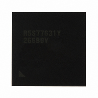
R5S77631Y266BGV Renesas Electronics America, R5S77631Y266BGV Datasheet - Page 1654

R5S77631Y266BGV
Manufacturer Part Number
R5S77631Y266BGV
Description
IC SUPERH MPU ROMLESS 499BGA
Manufacturer
Renesas Electronics America
Series
SuperH® SH7780r
Datasheet
1.R5S77631Y266BGV.pdf
(2056 pages)
Specifications of R5S77631Y266BGV
Core Processor
SH-4A
Core Size
32-Bit
Speed
266MHz
Connectivity
Audio Codec, I²C, MMC, SCI, SIM, SIO, SSI, USB
Peripherals
DMA, LCD, POR, WDT
Number Of I /o
107
Program Memory Type
ROMless
Ram Size
16K x 8
Voltage - Supply (vcc/vdd)
1.15 V ~ 1.35 V
Data Converters
A/D 4x10b; D/A 2x8b
Oscillator Type
External
Operating Temperature
-20°C ~ 75°C
Package / Case
499-BGA
Lead Free Status / RoHS Status
Lead free / RoHS Compliant
Eeprom Size
-
Program Memory Size
-
Available stocks
Company
Part Number
Manufacturer
Quantity
Price
Company:
Part Number:
R5S77631Y266BGV
Manufacturer:
Renesas Electronics America
Quantity:
10 000
- Current page: 1654 of 2056
- Download datasheet (10Mb)
Section 36 USB Function Controller (USBF)
36.10
36.10.1 Setup Data Reception
The following points should be noted on the EP0s data register (EPDR0s) in which reception of 8-
byte setup data is performed.
1. Since the setup command must be received in the USB, writing from the USB bus side is prior
2. EPDR0s must be read in 8-byte units. If reading is suspended while it is in progress, data
36.10.2 FIFO Clear
When the USB cable is disconnected during communication, data which is receiving or
transmitting may remain in the FIFO. Therefore the FIFO must be cleared immediately after
connecting the USB cable again.
Note that the FIFO in which data is receiving from the host or transmitting to the host must not be
cleared.
36.10.3 Overreading/Overwriting of Data Register
The following points should be noted when the data register of the USBF is read from or written
to.
Receive Data Register: The receive data register must not read data which is more than valid
receive data bytes. That is, data which is more than bytes indicated in the receive data size register
must not be read. In case of the receive data register which has the dual FIFO buffer, the
maximum number of data which can be read in a single time is maximum packet size. Write 1 to
TRG after data in the current valid buffer is read. This writing switches the FIFO buffer. Then, the
new number of bytes is reflected in the receive data size and the next data can be read.
Transmit Data Register: The transmit data register must not write data which is more than
maximum packet size. In case of the transmit data register which has the dual FIFO buffer, the
maximum number of data which can be written in a single time is maximum packet size. Write 1
to TRG/PKTE after data is written. This writing switches the FIFO buffer. Then, the next data can
be written to another buffer. Therefore data must not be written in both buffers in a single time.
Rev. 2.00 May 22, 2009 Page 1584 of 1982
REJ09B0256-0200
to reading from the CPU side. While the CPU reads data after completion of reception and
reception of the next setup command is started, reading from the CPU side is forcibly invalid.
Therefore a value to be read after starting reception is undefined.
received in the next setup cannot be read successfully.
Usage Notes
Related parts for R5S77631Y266BGV
Image
Part Number
Description
Manufacturer
Datasheet
Request
R

Part Number:
Description:
KIT STARTER FOR M16C/29
Manufacturer:
Renesas Electronics America
Datasheet:

Part Number:
Description:
KIT STARTER FOR R8C/2D
Manufacturer:
Renesas Electronics America
Datasheet:

Part Number:
Description:
R0K33062P STARTER KIT
Manufacturer:
Renesas Electronics America
Datasheet:

Part Number:
Description:
KIT STARTER FOR R8C/23 E8A
Manufacturer:
Renesas Electronics America
Datasheet:

Part Number:
Description:
KIT STARTER FOR R8C/25
Manufacturer:
Renesas Electronics America
Datasheet:

Part Number:
Description:
KIT STARTER H8S2456 SHARPE DSPLY
Manufacturer:
Renesas Electronics America
Datasheet:

Part Number:
Description:
KIT STARTER FOR R8C38C
Manufacturer:
Renesas Electronics America
Datasheet:

Part Number:
Description:
KIT STARTER FOR R8C35C
Manufacturer:
Renesas Electronics America
Datasheet:

Part Number:
Description:
KIT STARTER FOR R8CL3AC+LCD APPS
Manufacturer:
Renesas Electronics America
Datasheet:

Part Number:
Description:
KIT STARTER FOR RX610
Manufacturer:
Renesas Electronics America
Datasheet:

Part Number:
Description:
KIT STARTER FOR R32C/118
Manufacturer:
Renesas Electronics America
Datasheet:

Part Number:
Description:
KIT DEV RSK-R8C/26-29
Manufacturer:
Renesas Electronics America
Datasheet:

Part Number:
Description:
KIT STARTER FOR SH7124
Manufacturer:
Renesas Electronics America
Datasheet:

Part Number:
Description:
KIT STARTER FOR H8SX/1622
Manufacturer:
Renesas Electronics America
Datasheet:

Part Number:
Description:
KIT DEV FOR SH7203
Manufacturer:
Renesas Electronics America
Datasheet:


