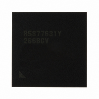
R5S77631Y266BGV Renesas Electronics America, R5S77631Y266BGV Datasheet - Page 1738

R5S77631Y266BGV
Manufacturer Part Number
R5S77631Y266BGV
Description
IC SUPERH MPU ROMLESS 499BGA
Manufacturer
Renesas Electronics America
Series
SuperH® SH7780r
Datasheet
1.R5S77631Y266BGV.pdf
(2056 pages)
Specifications of R5S77631Y266BGV
Core Processor
SH-4A
Core Size
32-Bit
Speed
266MHz
Connectivity
Audio Codec, I²C, MMC, SCI, SIM, SIO, SSI, USB
Peripherals
DMA, LCD, POR, WDT
Number Of I /o
107
Program Memory Type
ROMless
Ram Size
16K x 8
Voltage - Supply (vcc/vdd)
1.15 V ~ 1.35 V
Data Converters
A/D 4x10b; D/A 2x8b
Oscillator Type
External
Operating Temperature
-20°C ~ 75°C
Package / Case
499-BGA
Lead Free Status / RoHS Status
Lead free / RoHS Compliant
Eeprom Size
-
Program Memory Size
-
Available stocks
Company
Part Number
Manufacturer
Quantity
Price
Company:
Part Number:
R5S77631Y266BGV
Manufacturer:
Renesas Electronics America
Quantity:
10 000
- Current page: 1738 of 2056
- Download datasheet (10Mb)
Section 38 A/D Converter
38.4.3
In scan mode, A/D conversion is continuously repeated for the selected channels until the ADST
bit (bit 13) is cleared to 0. The A/D conversion results are transferred for storage to the ADDR that
corresponds to the channel. This mode is suitable for systems that continuously monitor analog
inputs to multiple channels (or a single channel). A/D conversion starts with the first channel
(AN0) when the ADST bit of the A/D control/status register (ADCSR) is set to 1 by software.
When multiple channels are selected, after A/D conversion for channel n ends, A/D conversion for
channel (n + 1) starts immediately.
A/D conversion is continuously repeated for the selected channels until the ADST bit is cleared to
0. The conversion results are transferred for storage to the ADDR that corresponds to the channel.
When setting the A/D control/status register (ADCSR) or switching the analog input channel
during A/D conversion, first clear the ADST bit to 0 to halt A/D conversion in order to avoid
malfunction. After the change has been made, setting the ADST bit to 1 selects the first channel
and A/D conversion is resumed.
Typical operations when three channels (AN0 to AN2) are selected in scan mode are described
below. Figure 38.4 shows a timing diagram for this example.
1. Select scan mode as the operating mode (MDS[1:0] = 11) and AN0 to AN2 as the input
2. A/D conversion of the first channel (AN0) starts. When A/D conversion ends, the result is
3. A/D conversion proceeds in the same way up to the third channel (AN2).
4. When A/D conversion of all selected channels (AN0 to AN2) is completed, the ADF bit is set
5. While the ADST bit is set to 1, steps 2 to 4 above are repeated.
Rev. 2.00 May 22, 2009 Page 1668 of 1982
REJ09B0256-0200
channels (CH[2:0] = 010). Then start A/D conversion (ADST = 1).
transferred into ADDRA. Next, the second channel (AN1) is selected automatically and A/D
conversion starts.
to 1, the first channel (AN0) is selected again, and A/D conversion is consecutively performed.
(In multi mode, A/D conversion ends when the selected channels have been cycled through.
However, in scan mode, after the selected channels have been cycled through, A/D conversion
starts again from the first channel and is consecutively repeated.)
If the ADIE bit is set to 1 at this time, an ADI interrupt is generated after A/D conversion ends.
When the ADST bit is cleared to 0, A/D conversion stops. After that, if the ADST bit is set to
1, A/D conversion starts again from the first channel (AN0).
Scan Mode (MDS1 = 1, MDS0 = 1)
Related parts for R5S77631Y266BGV
Image
Part Number
Description
Manufacturer
Datasheet
Request
R

Part Number:
Description:
KIT STARTER FOR M16C/29
Manufacturer:
Renesas Electronics America
Datasheet:

Part Number:
Description:
KIT STARTER FOR R8C/2D
Manufacturer:
Renesas Electronics America
Datasheet:

Part Number:
Description:
R0K33062P STARTER KIT
Manufacturer:
Renesas Electronics America
Datasheet:

Part Number:
Description:
KIT STARTER FOR R8C/23 E8A
Manufacturer:
Renesas Electronics America
Datasheet:

Part Number:
Description:
KIT STARTER FOR R8C/25
Manufacturer:
Renesas Electronics America
Datasheet:

Part Number:
Description:
KIT STARTER H8S2456 SHARPE DSPLY
Manufacturer:
Renesas Electronics America
Datasheet:

Part Number:
Description:
KIT STARTER FOR R8C38C
Manufacturer:
Renesas Electronics America
Datasheet:

Part Number:
Description:
KIT STARTER FOR R8C35C
Manufacturer:
Renesas Electronics America
Datasheet:

Part Number:
Description:
KIT STARTER FOR R8CL3AC+LCD APPS
Manufacturer:
Renesas Electronics America
Datasheet:

Part Number:
Description:
KIT STARTER FOR RX610
Manufacturer:
Renesas Electronics America
Datasheet:

Part Number:
Description:
KIT STARTER FOR R32C/118
Manufacturer:
Renesas Electronics America
Datasheet:

Part Number:
Description:
KIT DEV RSK-R8C/26-29
Manufacturer:
Renesas Electronics America
Datasheet:

Part Number:
Description:
KIT STARTER FOR SH7124
Manufacturer:
Renesas Electronics America
Datasheet:

Part Number:
Description:
KIT STARTER FOR H8SX/1622
Manufacturer:
Renesas Electronics America
Datasheet:

Part Number:
Description:
KIT DEV FOR SH7203
Manufacturer:
Renesas Electronics America
Datasheet:


