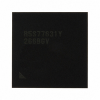
R5S77631Y266BGV Renesas Electronics America, R5S77631Y266BGV Datasheet - Page 1871

R5S77631Y266BGV
Manufacturer Part Number
R5S77631Y266BGV
Description
IC SUPERH MPU ROMLESS 499BGA
Manufacturer
Renesas Electronics America
Series
SuperH® SH7780r
Datasheet
1.R5S77631Y266BGV.pdf
(2056 pages)
Specifications of R5S77631Y266BGV
Core Processor
SH-4A
Core Size
32-Bit
Speed
266MHz
Connectivity
Audio Codec, I²C, MMC, SCI, SIM, SIO, SSI, USB
Peripherals
DMA, LCD, POR, WDT
Number Of I /o
107
Program Memory Type
ROMless
Ram Size
16K x 8
Voltage - Supply (vcc/vdd)
1.15 V ~ 1.35 V
Data Converters
A/D 4x10b; D/A 2x8b
Oscillator Type
External
Operating Temperature
-20°C ~ 75°C
Package / Case
499-BGA
Lead Free Status / RoHS Status
Lead free / RoHS Compliant
Eeprom Size
-
Program Memory Size
-
Available stocks
Company
Part Number
Manufacturer
Quantity
Price
Company:
Part Number:
R5S77631Y266BGV
Manufacturer:
Renesas Electronics America
Quantity:
10 000
- Current page: 1871 of 2056
- Download datasheet (10Mb)
42.2
Table 42.1 shows the pin configuration for the H-UDI.
Table 42.1 Pin Configuration
Notes: 1. This pin is pulled up in this LSI. When using interrupts or resets via the H-UDI or
Pin Name
TCK
TMS
TRST*
TDI
TDO
ASEBRK/
BRKACK
AUDSYNC,
AUDCK,
AUDATA3 to
AUDATA0
MPMD
2
2. When using interrupts or resets via the H-UDI or emulator, the TRST pin should be
Input/Output Pins
emulator, the use of external pull-up resistors will not cause any problem.
designed so that it can be controlled independently and can be controlled to retain low
level while the PRESET pin is asserted at a power-on reset.
Function
Clock
Mode
Reset
Data input
Data output Output
Emulator
Emulator
Chip-mode Input
Input
I/O
Input
Input
Input
I/O
Output
Description
Functions as the serial clock input pin stipulated in
the JTAG standard. Data input to the H-UDI via the
TDI pin or data Output via the TDO pin is performed
in synchronization with this signal.
Mode Select Input
Changing this signal in synchronization with the TCK
signal determines the significance of data input via
the TDI pin. Its protocol conforms to the JTAG
standard (IEEE standard 1149.1).
H-UDI Reset Input
This signal is received asynchronously with a TCK
signal. Asserting this signal resets the JTAG interface
circuit. When a power is supplied, the TRST pin
should be asserted for a given period regardless of
whether or not the JTAG function is used, which
differs from the JTAG standard.
Data Input
Data is sent to the H-UDI by changing this signal in
synchronization with the TCK signal.
Data Output
Data is read from the H-UDI in synchronization with
the TCK signal.
Pins for an emulator
Pins for an emulator
Selects the operation mode of this LSI, whether
emulation support mode (Low level) or LSI operation
mode (High level).
Section 42 User Debugging Interface (H-UDI)
Rev. 2.00 May 22, 2009 Page 1801 of 1982
REJ09B0256-0200
When Not
in Use
Open*
Open*
Fixed to
ground or
connected to
the PRESET
pin*
Open*
Open
Open*
Open
Open
3
1
1
1
1
Related parts for R5S77631Y266BGV
Image
Part Number
Description
Manufacturer
Datasheet
Request
R

Part Number:
Description:
KIT STARTER FOR M16C/29
Manufacturer:
Renesas Electronics America
Datasheet:

Part Number:
Description:
KIT STARTER FOR R8C/2D
Manufacturer:
Renesas Electronics America
Datasheet:

Part Number:
Description:
R0K33062P STARTER KIT
Manufacturer:
Renesas Electronics America
Datasheet:

Part Number:
Description:
KIT STARTER FOR R8C/23 E8A
Manufacturer:
Renesas Electronics America
Datasheet:

Part Number:
Description:
KIT STARTER FOR R8C/25
Manufacturer:
Renesas Electronics America
Datasheet:

Part Number:
Description:
KIT STARTER H8S2456 SHARPE DSPLY
Manufacturer:
Renesas Electronics America
Datasheet:

Part Number:
Description:
KIT STARTER FOR R8C38C
Manufacturer:
Renesas Electronics America
Datasheet:

Part Number:
Description:
KIT STARTER FOR R8C35C
Manufacturer:
Renesas Electronics America
Datasheet:

Part Number:
Description:
KIT STARTER FOR R8CL3AC+LCD APPS
Manufacturer:
Renesas Electronics America
Datasheet:

Part Number:
Description:
KIT STARTER FOR RX610
Manufacturer:
Renesas Electronics America
Datasheet:

Part Number:
Description:
KIT STARTER FOR R32C/118
Manufacturer:
Renesas Electronics America
Datasheet:

Part Number:
Description:
KIT DEV RSK-R8C/26-29
Manufacturer:
Renesas Electronics America
Datasheet:

Part Number:
Description:
KIT STARTER FOR SH7124
Manufacturer:
Renesas Electronics America
Datasheet:

Part Number:
Description:
KIT STARTER FOR H8SX/1622
Manufacturer:
Renesas Electronics America
Datasheet:

Part Number:
Description:
KIT DEV FOR SH7203
Manufacturer:
Renesas Electronics America
Datasheet:


