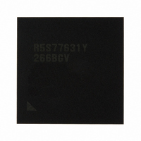
R5S77631Y266BGV Renesas Electronics America, R5S77631Y266BGV Datasheet - Page 260

R5S77631Y266BGV
Manufacturer Part Number
R5S77631Y266BGV
Description
IC SUPERH MPU ROMLESS 499BGA
Manufacturer
Renesas Electronics America
Series
SuperH® SH7780r
Datasheet
1.R5S77631Y266BGV.pdf
(2056 pages)
Specifications of R5S77631Y266BGV
Core Processor
SH-4A
Core Size
32-Bit
Speed
266MHz
Connectivity
Audio Codec, I²C, MMC, SCI, SIM, SIO, SSI, USB
Peripherals
DMA, LCD, POR, WDT
Number Of I /o
107
Program Memory Type
ROMless
Ram Size
16K x 8
Voltage - Supply (vcc/vdd)
1.15 V ~ 1.35 V
Data Converters
A/D 4x10b; D/A 2x8b
Oscillator Type
External
Operating Temperature
-20°C ~ 75°C
Package / Case
499-BGA
Lead Free Status / RoHS Status
Lead free / RoHS Compliant
Eeprom Size
-
Program Memory Size
-
Available stocks
Company
Part Number
Manufacturer
Quantity
Price
Company:
Part Number:
R5S77631Y266BGV
Manufacturer:
Renesas Electronics America
Quantity:
10 000
- Current page: 260 of 2056
- Download datasheet (10Mb)
Section 7 Caches
• Data array
• LRU
7.2
The following registers are related to cache.
Table 7.3
Note:
Table 7.4
Rev. 2.00 May 22, 2009 Page 190 of 1982
REJ09B0256-0200
Register Name
Cache control register
Queue address control register 0
Queue address control register 1
On-chip memory control register
Register Name
Cache control register
Queue address control register 0 QACR0
Queue address control register 1 QACR1
On-chip memory control register
The data field holds 32 bytes (256 bits) of data per cache line. The data array is not initialized
by a power-on or manual reset.
In a 4-way set-associative method, up to 4 items of data can be registered in the cache at each
entry address. When an entry is registered, the LRU bit indicates which of the 4 ways it is to be
registered in. The LRU mechanism uses 6 bits of each entry, and its usage is controlled by
hardware. The LRU (least-recently-used) algorithm is used for way selection, and selects the
less recently accessed way. The LRU bits are initialized to 0 by a power-on reset but not by a
manual reset. The LRU bits cannot be read from or written to by software.
*
Register Descriptions
These P4 addresses are for the P4 area in the virtual address space. These area 7
addresses are accessed from area 7 in the physical address space by means of the
TLB.
Register Configuration
Register States in Each Processing State
Abbreviation
CCR
RAMCR
Abbreviation R/W
CCR
QACR0
QACR1
RAMCR
Power-on Reset Manual Reset
H
Undefined
Undefined
H
R/W
R/W
R/W
R/W
'
'
0000 0000
0000 0000
P4 Address*
H
H
H
H
'
'
'
'
FF00 001C
FF00 0038
FF00 003C
FF00 0074
H
Undefined
Undefined
H
'
'
0000 0000
0000 0000
Area 7 Address*
H
H
H
H
'
'
'
'
1F00 001C
1F00 0038
1F00 003C
1F00 0074
Sleep
Retained
Retained
Retained
Retained
Size
32
32
32
32
Standby
Retained
Retained
Retained
Retained
Related parts for R5S77631Y266BGV
Image
Part Number
Description
Manufacturer
Datasheet
Request
R

Part Number:
Description:
KIT STARTER FOR M16C/29
Manufacturer:
Renesas Electronics America
Datasheet:

Part Number:
Description:
KIT STARTER FOR R8C/2D
Manufacturer:
Renesas Electronics America
Datasheet:

Part Number:
Description:
R0K33062P STARTER KIT
Manufacturer:
Renesas Electronics America
Datasheet:

Part Number:
Description:
KIT STARTER FOR R8C/23 E8A
Manufacturer:
Renesas Electronics America
Datasheet:

Part Number:
Description:
KIT STARTER FOR R8C/25
Manufacturer:
Renesas Electronics America
Datasheet:

Part Number:
Description:
KIT STARTER H8S2456 SHARPE DSPLY
Manufacturer:
Renesas Electronics America
Datasheet:

Part Number:
Description:
KIT STARTER FOR R8C38C
Manufacturer:
Renesas Electronics America
Datasheet:

Part Number:
Description:
KIT STARTER FOR R8C35C
Manufacturer:
Renesas Electronics America
Datasheet:

Part Number:
Description:
KIT STARTER FOR R8CL3AC+LCD APPS
Manufacturer:
Renesas Electronics America
Datasheet:

Part Number:
Description:
KIT STARTER FOR RX610
Manufacturer:
Renesas Electronics America
Datasheet:

Part Number:
Description:
KIT STARTER FOR R32C/118
Manufacturer:
Renesas Electronics America
Datasheet:

Part Number:
Description:
KIT DEV RSK-R8C/26-29
Manufacturer:
Renesas Electronics America
Datasheet:

Part Number:
Description:
KIT STARTER FOR SH7124
Manufacturer:
Renesas Electronics America
Datasheet:

Part Number:
Description:
KIT STARTER FOR H8SX/1622
Manufacturer:
Renesas Electronics America
Datasheet:

Part Number:
Description:
KIT DEV FOR SH7203
Manufacturer:
Renesas Electronics America
Datasheet:


