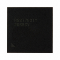
R5S77631Y266BGV Renesas Electronics America, R5S77631Y266BGV Datasheet - Page 48

R5S77631Y266BGV
Manufacturer Part Number
R5S77631Y266BGV
Description
IC SUPERH MPU ROMLESS 499BGA
Manufacturer
Renesas Electronics America
Series
SuperH® SH7780r
Datasheet
1.R5S77631Y266BGV.pdf
(2056 pages)
Specifications of R5S77631Y266BGV
Core Processor
SH-4A
Core Size
32-Bit
Speed
266MHz
Connectivity
Audio Codec, I²C, MMC, SCI, SIM, SIO, SSI, USB
Peripherals
DMA, LCD, POR, WDT
Number Of I /o
107
Program Memory Type
ROMless
Ram Size
16K x 8
Voltage - Supply (vcc/vdd)
1.15 V ~ 1.35 V
Data Converters
A/D 4x10b; D/A 2x8b
Oscillator Type
External
Operating Temperature
-20°C ~ 75°C
Package / Case
499-BGA
Lead Free Status / RoHS Status
Lead free / RoHS Compliant
Eeprom Size
-
Program Memory Size
-
Available stocks
Company
Part Number
Manufacturer
Quantity
Price
Company:
Part Number:
R5S77631Y266BGV
Manufacturer:
Renesas Electronics America
Quantity:
10 000
- Current page: 48 of 2056
- Download datasheet (10Mb)
Figure 22.4 Example of Use of Alarm Function......................................................................... 782
Figure 22.5 Example of Crystal Oscillator Circuit Connection.................................................. 784
Section 23 Gigabit Ethernet Controller (GETHER)
Figure 23.1 Configuration of GETHER ..................................................................................... 786
Figure 23.2 GETHER Data Path and Various Settings .............................................................. 940
Figure 23.3 Relationship between Transmit Descriptor and Transmit Buffer............................ 942
Figure 23.4 Relationship between Receive Descriptor and Receive Buffer ............................... 948
Figure 23.5 Relationship between Transmit Descriptor and Transmit Buffer............................ 954
Figure 23.6 Relationship between Receive Descriptor and Receive Buffer ............................... 955
Figure 23.7 Relationship between Transmit/Receive Descriptor and Descriptor Pointing
Registers.................................................................................................................. 957
Figure 23.8 Sample Transmission Flowchart (Single-Frame/Two-Description)........................ 960
Figure 23.9 E-MAC Transmitter State Transitions..................................................................... 962
Figure 23.10 E-MAC Receiver State Transitions ....................................................................... 965
Figure 23.11 Sample Reception Flowchart (Single-Frame/Two-Descriptor)............................. 967
Figure 23.12 E-DMAC Operation after Transmit Error ............................................................. 973
Figure 23.13 E-DMAC Operation after Receive Error............................................................... 974
Figure 23.14 Padding Insertion in Receive Data ........................................................................ 975
Figure 23.15 Outlines of Qtag Additional Functions.................................................................. 984
Figure 23.16 Comparison of Normal Ethernet Frame and IEEE802.1Q Frame (with Qtag)...... 985
Figure 23.17 MII Frame Transmit Timing (Normal Transmission) ........................................... 986
Figure 23.18 MII Frame Transmit Timing (Collision) ............................................................... 986
Figure 23.19 MII Frame Transmit Timing (Transmit Error) ...................................................... 987
Figure 23.20 MII Frame Receive Timing (Normal Reception) .................................................. 987
Figure 23.21 MII Frame Receive Timing (Reception Error (1)) ................................................ 987
Figure 23.22 MII Fame Receive Timing (Reception Error (2)).................................................. 987
Figure 23.23 GMII/MII Fame Receive Timing (Normal Reception) ......................................... 988
Figure 23.24 GMII/MII Fame Receive Timing (with Carrier Extension) .................................. 988
Figure 23.25 GMII/MII Fame Receive Timing (Burst Reception)............................................. 988
Figure 23.26 GMII/MII Fame Receive Timing (Reception Error) ............................................. 989
Figure 23.27 GMII/MII Fame Receive Timing (Error with Carrier Extension) ......................... 989
Figure 23.28 GMII/MII Fame Receive Timing (False Carrier Indication)................................. 989
Figure 23.29 RMII Fame Receive Timing (Normal 100-Mbps Reception) ............................... 990
Figure 23.30 RMII Fame Receive Timing
(100-Mbps Reception with Illegal Carrier Detected) ............................................ 990
Figure 23.31 RMII Fame Transmit Timing (Normal 100-Mbps Transmission)......................... 990
Figure 23.32 MII Management Frame Format ........................................................................... 991
Figure 23.33 1-Bit Data Write Flowchart................................................................................... 992
Figure 23.34 Bus Release Flowchart (TA in Read in Figure 23.33)........................................... 992
Figure 23.35 1-Bit Data Read Flowchart.................................................................................... 993
Rev. 2.00 May 22, 2009 Page xlvi of lxviii
Related parts for R5S77631Y266BGV
Image
Part Number
Description
Manufacturer
Datasheet
Request
R

Part Number:
Description:
KIT STARTER FOR M16C/29
Manufacturer:
Renesas Electronics America
Datasheet:

Part Number:
Description:
KIT STARTER FOR R8C/2D
Manufacturer:
Renesas Electronics America
Datasheet:

Part Number:
Description:
R0K33062P STARTER KIT
Manufacturer:
Renesas Electronics America
Datasheet:

Part Number:
Description:
KIT STARTER FOR R8C/23 E8A
Manufacturer:
Renesas Electronics America
Datasheet:

Part Number:
Description:
KIT STARTER FOR R8C/25
Manufacturer:
Renesas Electronics America
Datasheet:

Part Number:
Description:
KIT STARTER H8S2456 SHARPE DSPLY
Manufacturer:
Renesas Electronics America
Datasheet:

Part Number:
Description:
KIT STARTER FOR R8C38C
Manufacturer:
Renesas Electronics America
Datasheet:

Part Number:
Description:
KIT STARTER FOR R8C35C
Manufacturer:
Renesas Electronics America
Datasheet:

Part Number:
Description:
KIT STARTER FOR R8CL3AC+LCD APPS
Manufacturer:
Renesas Electronics America
Datasheet:

Part Number:
Description:
KIT STARTER FOR RX610
Manufacturer:
Renesas Electronics America
Datasheet:

Part Number:
Description:
KIT STARTER FOR R32C/118
Manufacturer:
Renesas Electronics America
Datasheet:

Part Number:
Description:
KIT DEV RSK-R8C/26-29
Manufacturer:
Renesas Electronics America
Datasheet:

Part Number:
Description:
KIT STARTER FOR SH7124
Manufacturer:
Renesas Electronics America
Datasheet:

Part Number:
Description:
KIT STARTER FOR H8SX/1622
Manufacturer:
Renesas Electronics America
Datasheet:

Part Number:
Description:
KIT DEV FOR SH7203
Manufacturer:
Renesas Electronics America
Datasheet:


