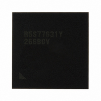
R5S77631Y266BGV Renesas Electronics America, R5S77631Y266BGV Datasheet - Page 534

R5S77631Y266BGV
Manufacturer Part Number
R5S77631Y266BGV
Description
IC SUPERH MPU ROMLESS 499BGA
Manufacturer
Renesas Electronics America
Series
SuperH® SH7780r
Datasheet
1.R5S77631Y266BGV.pdf
(2056 pages)
Specifications of R5S77631Y266BGV
Core Processor
SH-4A
Core Size
32-Bit
Speed
266MHz
Connectivity
Audio Codec, I²C, MMC, SCI, SIM, SIO, SSI, USB
Peripherals
DMA, LCD, POR, WDT
Number Of I /o
107
Program Memory Type
ROMless
Ram Size
16K x 8
Voltage - Supply (vcc/vdd)
1.15 V ~ 1.35 V
Data Converters
A/D 4x10b; D/A 2x8b
Oscillator Type
External
Operating Temperature
-20°C ~ 75°C
Package / Case
499-BGA
Lead Free Status / RoHS Status
Lead free / RoHS Compliant
Eeprom Size
-
Program Memory Size
-
Available stocks
Company
Part Number
Manufacturer
Quantity
Price
Company:
Part Number:
R5S77631Y266BGV
Manufacturer:
Renesas Electronics America
Quantity:
10 000
- Current page: 534 of 2056
- Download datasheet (10Mb)
Section 13 PCI Controller (PCIC)
(3)
The PCI command register provides coarse control over a device's ability to generate and respond
to PCI cycles. When 0 is written to this register, the device is logically disconnected from the PCI
bus for all accesses except configuration accesses.
Rev. 2.00 May 22, 2009 Page 464 of 1982
REJ09B0256-0200
Initial value:
Bit
15 to 10
9
8
7
PCI R/W:
SH R/W:
PCI Command Register (PCICMD)
Bit:
Bit Name
FBBE
SERRE
WCC
15
R
R
0
14
R
R
0
Initial
Value
All 0
0
0
1
13
R
R
0
12
R
R
0
R/W
SH: R
PCI: R
SH: R
PCI: R
SH: R/W
PCI: R/W
SH: R/W
PCI: R/W
11
R
R
0
10
R
R
0
Description
Reserved
These bits are always read as 0. The write value
should always be 0.
PCI Fast Back-to-Back Enable
Controls whether or not a master can do fast back-to-
back transactions to different device.
0: Fast back-to-back transactions are only allowed to
the same target
1: Master is allowed to generate fast back-to-back
transactions to different targets (not supported)
PCI SERR Output Control
Controls the SERR output.
0: SERR output disabled
1: SERR output enabled
Wait Cycle Control
Controls the address/data stepping.
When WCC = 1, both an address and data for a master
write, only an address for a master read, and only data
for a target read are output for at least two clock cycles.
0: Address/data stepping control disabled
1: Address/data stepping control enabled
FBBE
R
R
9
0
SERRE
R/W
R/W
8
0
WCC
R/W
R/W
7
1
R/W
R/W
PER
6
0
VGAPS
R
R
5
0
MWIE
R
R
4
0
SC
R
R
3
0
R/W
R/W
BM
2
0
R/W
R/W
MS
1
0
R/W
R/W
IOS
0
0
Related parts for R5S77631Y266BGV
Image
Part Number
Description
Manufacturer
Datasheet
Request
R

Part Number:
Description:
KIT STARTER FOR M16C/29
Manufacturer:
Renesas Electronics America
Datasheet:

Part Number:
Description:
KIT STARTER FOR R8C/2D
Manufacturer:
Renesas Electronics America
Datasheet:

Part Number:
Description:
R0K33062P STARTER KIT
Manufacturer:
Renesas Electronics America
Datasheet:

Part Number:
Description:
KIT STARTER FOR R8C/23 E8A
Manufacturer:
Renesas Electronics America
Datasheet:

Part Number:
Description:
KIT STARTER FOR R8C/25
Manufacturer:
Renesas Electronics America
Datasheet:

Part Number:
Description:
KIT STARTER H8S2456 SHARPE DSPLY
Manufacturer:
Renesas Electronics America
Datasheet:

Part Number:
Description:
KIT STARTER FOR R8C38C
Manufacturer:
Renesas Electronics America
Datasheet:

Part Number:
Description:
KIT STARTER FOR R8C35C
Manufacturer:
Renesas Electronics America
Datasheet:

Part Number:
Description:
KIT STARTER FOR R8CL3AC+LCD APPS
Manufacturer:
Renesas Electronics America
Datasheet:

Part Number:
Description:
KIT STARTER FOR RX610
Manufacturer:
Renesas Electronics America
Datasheet:

Part Number:
Description:
KIT STARTER FOR R32C/118
Manufacturer:
Renesas Electronics America
Datasheet:

Part Number:
Description:
KIT DEV RSK-R8C/26-29
Manufacturer:
Renesas Electronics America
Datasheet:

Part Number:
Description:
KIT STARTER FOR SH7124
Manufacturer:
Renesas Electronics America
Datasheet:

Part Number:
Description:
KIT STARTER FOR H8SX/1622
Manufacturer:
Renesas Electronics America
Datasheet:

Part Number:
Description:
KIT DEV FOR SH7203
Manufacturer:
Renesas Electronics America
Datasheet:


