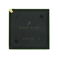
MPC561MZP56 Freescale, MPC561MZP56 Datasheet - Page 1034

MPC561MZP56
Manufacturer Part Number
MPC561MZP56
Description
Manufacturer
Freescale
Datasheet
1.MPC561MZP56.pdf
(1420 pages)
Specifications of MPC561MZP56
Cpu Family
MPC56x
Device Core
PowerPC
Device Core Size
32b
Frequency (max)
56MHz
Interface Type
QSPI/SCI/SPI/UART
Total Internal Ram Size
32KB
# I/os (max)
56
Number Of Timers - General Purpose
22
Operating Supply Voltage (typ)
2.6/5V
Operating Supply Voltage (max)
2.7/5.25V
Operating Supply Voltage (min)
2.5/4.75V
On-chip Adc
2(32-chx10-bit)
Instruction Set Architecture
RISC
Operating Temp Range
-40C to 125C
Operating Temperature Classification
Automotive
Mounting
Surface Mount
Pin Count
388
Package Type
BGA
Program Memory Type
ROMLess
Program Memory Size
Not Required
Lead Free Status / RoHS Status
Not Compliant
Available stocks
Company
Part Number
Manufacturer
Quantity
Price
Company:
Part Number:
MPC561MZP56
Manufacturer:
Freescale Semiconductor
Quantity:
10 000
Company:
Part Number:
MPC561MZP56R2
Manufacturer:
Freescale Semiconductor
Quantity:
10 000
- Current page: 1034 of 1420
- Download datasheet (11Mb)
READI Module
L-bus data error conditions are signalled along with the transfer acknowledge for the access. L-bus data
error conditions may occur because of privilege violations, access to protected memory, etc. In such cases,
for a read access, the ERR bit of the UDI is set, and the DV bit in the UDI is reset at the termination of the
access. For a write access, an error public message (TCODE = 8) is transmitted (error code 0b00011).
24.10.6 Exception Sequences
The following cases are defined for sequences of the read/write protocol that differ from those described
in the above sections:
24.10.7 Secure Mode
For details refer to
24.10.8 Error Messages
24.10.8.1 Read/Write Access Error
An error message is sent out when an L-bus access error or data error on a write access occurs. The error
code within the error message indicates that an L-bus address or L-bus data error occurred. For other error
handling, see
24-66
•
•
•
1. If the SC bit is set to start READI read/write accesses, without valid values in the RWAD, then an
2. If a block access is in progress with all the cycles not yet completed, and the RWA is written to
3. When a block access is in progress with all the cycles not yet completed, writing the SC bit to 0 in
4. If a any type (single/block) of access is in progress with the cycles not yet completed, and system
5. If any type of (single/block) of access is requested while system is in reset, the device will send out
L-bus data phase error.
U-bus address phase error (for a L-bus to U-bus cycle).
U-bus data phase error (for a L-bus to U-bus cycle).
L-bus address error may occur, which is handled as described above.
again, (with or without modifications), then the block access is terminated at the boundary of the
nearest completed access. The resulting data is discarded and not written to the UDI. If a new
access has been programmed in the RWA register, then that access will start once the controller has
recovered.
RWA register will terminate the block access and device will send out device ready for
upload/download message.
reset occurs, the device will send out an error message. The access will be terminated and the SC
bit will be reset. Refer to
an error message. The access will not be started and the SC bit will be reset.
Section 24.10.5, “Error
Section 24.2.2,
MPC561/MPC563 Reference Manual, Rev. 1.2
Table
“Security.”
Handling.” For a list of error codes, refer to
24-20.
Table
Freescale Semiconductor
24-20.
Related parts for MPC561MZP56
Image
Part Number
Description
Manufacturer
Datasheet
Request
R

Part Number:
Description:
MPC5 1K0 5%
Manufacturer:
TE Connectivity
Datasheet:

Part Number:
Description:
MPC5 500R 5%
Manufacturer:
TE Connectivity
Datasheet:

Part Number:
Description:
MPC5 5K0 5%
Manufacturer:
Tyco Electronics
Datasheet:

Part Number:
Description:
MPC5 5R0 5%
Manufacturer:
Tyco Electronics
Datasheet:

Part Number:
Description:
MPC5 50K 5%
Manufacturer:
Tyco Electronics
Datasheet:

Part Number:
Description:
MPC5 1R0 5%
Manufacturer:
Tyco Electronics
Datasheet:

Part Number:
Description:
TOWER ELEVATOR BOARDS HARDWARE
Manufacturer:
Freescale Semiconductor
Datasheet:

Part Number:
Description:
TOWER SERIAL I/O HARDWARE
Manufacturer:
Freescale Semiconductor
Datasheet:

Part Number:
Description:
LCD MODULE FOR TWR SYSTEM
Manufacturer:
Freescale Semiconductor
Datasheet:

Part Number:
Description:
DAUGHTER LCD WVGA I.MX51
Manufacturer:
Freescale Semiconductor
Datasheet:

Part Number:
Description:
TOWER SYSTEM BOARD MPC5125
Manufacturer:
Freescale Semiconductor
Datasheet:


