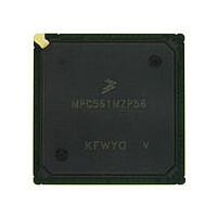
MPC561MZP56 Freescale, MPC561MZP56 Datasheet - Page 1084

MPC561MZP56
Manufacturer Part Number
MPC561MZP56
Description
Manufacturer
Freescale
Datasheet
1.MPC561MZP56.pdf
(1420 pages)
Specifications of MPC561MZP56
Cpu Family
MPC56x
Device Core
PowerPC
Device Core Size
32b
Frequency (max)
56MHz
Interface Type
QSPI/SCI/SPI/UART
Total Internal Ram Size
32KB
# I/os (max)
56
Number Of Timers - General Purpose
22
Operating Supply Voltage (typ)
2.6/5V
Operating Supply Voltage (max)
2.7/5.25V
Operating Supply Voltage (min)
2.5/4.75V
On-chip Adc
2(32-chx10-bit)
Instruction Set Architecture
RISC
Operating Temp Range
-40C to 125C
Operating Temperature Classification
Automotive
Mounting
Surface Mount
Pin Count
388
Package Type
BGA
Program Memory Type
ROMLess
Program Memory Size
Not Required
Lead Free Status / RoHS Status
Not Compliant
Available stocks
Company
Part Number
Manufacturer
Quantity
Price
Company:
Part Number:
MPC561MZP56
Manufacturer:
Freescale Semiconductor
Quantity:
10 000
Company:
Part Number:
MPC561MZP56R2
Manufacturer:
Freescale Semiconductor
Quantity:
10 000
- Current page: 1084 of 1420
- Download datasheet (11Mb)
IEEE 1149.1-Compliant Interface (JTAG)
9. Column Descriptions:
25.1.3
The MPC561/MPC563 JTAG implementation includes the public instructions (EXTEST,
SAMPLE/PRELOAD, and BYPASS), and also supports the CLAMP instruction. One additional public
instruction (HI-Z) provides the capability for disabling all device output drivers. The MPC561/MPC563
includes a 4-bit instruction register without parity consisting of a shift register with four parallel outputs.
Data is transferred from the shift register to the parallel outputs during the update-IR controller state. The
four bits are used to decode the five unique instructions listed in.
The parallel output of the instruction register is reset to all ones in the test-logic-reset controller state.
25-30
•r – resized cell instance
•Columns 1 through 8 are entries from the boundary-scan description from the BSDL file. The columns and formats for each
•Column 1: Defines the bit’s ordinal position in the boundary scan register. The shift register cell nearest TDO (i.e., first to be
•Column 2: References one of the three standard JTAG Cell Types (BC_4, BC_2, and BC_7) that are used for this JTAG cell
•Column 3: Lists the pin name (also called the PortID) for all pin-related cells. For JTAG control cells or data cells that have
•Column 4: Lists the BSDL pin function.
•Column 5: The “safe bit” column specifies the value that should be loaded into the capture (and update) flip-flop of a given
•Column 6: The “control cell” column identifies the cell number of the control cell that is associated with this data cell, and can
•Column 7: The “disable value” column gives the value that must be scanned into the control cell identified by the previous
•Column 8: The “disable result” column identifies a given signal value of the PortID if that signal can be disabled. The values
•Column 9: The “pin function” column indicates the normal system pin directionality. (– Input Only Pin, O – Output Only Pin,
•Column 10: The pad type column describes relevant characteristics about each pad type. See the Pad Type Keys in Note 5
of these entries are defined in the IEEE Std. 1149.1b-1994 Supplement to the IEEE Std. 1149.1-1990, IEEE Standard Test
Access Port and Boundary-Scan Architecture document. Descriptions of these columns are described below:
shifted in) is defined as bit 0; the last bit to be shifted in is 519.
in the MPC561/MPC563. See the IEEE Std. 1149.1-1990, IEEE Standard Test Access Port and Boundary-Scan Architecture
document for further description of these standard cell types.
been designated as “internal”, an asterisk, is shown in this column.
cell when board-level test generation software might otherwise choose a value randomly.
disable its output.
“control cell” (column 6) to disable the port named by the relevant portID.
shown specifies the condition of the driver of that signal when it is disabled.
I/O – Bidirectional I/O pin)
above.
Instruction Register
This preset state is equivalent to the BYPASS instruction.
1
B0 (LSB) is shifted first
B3
0
0
0
0
0
MPC561/MPC563 Reference Manual, Rev. 1.2
Table 25-3. Instruction Decoding
B2
X
0
0
1
1
Code
B1
0
0
1
0
0
NOTE
B0
X
0
1
0
1
1
CLAMP and BYPASS
SAMPLE/PRELOAD
Instruction
EXTEST
BYPASS
HI-Z
Freescale Semiconductor
Related parts for MPC561MZP56
Image
Part Number
Description
Manufacturer
Datasheet
Request
R

Part Number:
Description:
MPC5 1K0 5%
Manufacturer:
TE Connectivity
Datasheet:

Part Number:
Description:
MPC5 500R 5%
Manufacturer:
TE Connectivity
Datasheet:

Part Number:
Description:
MPC5 5K0 5%
Manufacturer:
Tyco Electronics
Datasheet:

Part Number:
Description:
MPC5 5R0 5%
Manufacturer:
Tyco Electronics
Datasheet:

Part Number:
Description:
MPC5 50K 5%
Manufacturer:
Tyco Electronics
Datasheet:

Part Number:
Description:
MPC5 1R0 5%
Manufacturer:
Tyco Electronics
Datasheet:

Part Number:
Description:
TOWER ELEVATOR BOARDS HARDWARE
Manufacturer:
Freescale Semiconductor
Datasheet:

Part Number:
Description:
TOWER SERIAL I/O HARDWARE
Manufacturer:
Freescale Semiconductor
Datasheet:

Part Number:
Description:
LCD MODULE FOR TWR SYSTEM
Manufacturer:
Freescale Semiconductor
Datasheet:

Part Number:
Description:
DAUGHTER LCD WVGA I.MX51
Manufacturer:
Freescale Semiconductor
Datasheet:

Part Number:
Description:
TOWER SYSTEM BOARD MPC5125
Manufacturer:
Freescale Semiconductor
Datasheet:


