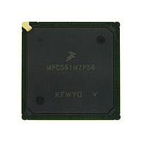
MPC561MZP56 Freescale, MPC561MZP56 Datasheet - Page 312

MPC561MZP56
Manufacturer Part Number
MPC561MZP56
Description
Manufacturer
Freescale
Datasheet
1.MPC561MZP56.pdf
(1420 pages)
Specifications of MPC561MZP56
Cpu Family
MPC56x
Device Core
PowerPC
Device Core Size
32b
Frequency (max)
56MHz
Interface Type
QSPI/SCI/SPI/UART
Total Internal Ram Size
32KB
# I/os (max)
56
Number Of Timers - General Purpose
22
Operating Supply Voltage (typ)
2.6/5V
Operating Supply Voltage (max)
2.7/5.25V
Operating Supply Voltage (min)
2.5/4.75V
On-chip Adc
2(32-chx10-bit)
Instruction Set Architecture
RISC
Operating Temp Range
-40C to 125C
Operating Temperature Classification
Automotive
Mounting
Surface Mount
Pin Count
388
Package Type
BGA
Program Memory Type
ROMLess
Program Memory Size
Not Required
Lead Free Status / RoHS Status
Not Compliant
Available stocks
Company
Part Number
Manufacturer
Quantity
Price
Company:
Part Number:
MPC561MZP56
Manufacturer:
Freescale Semiconductor
Quantity:
10 000
Company:
Part Number:
MPC561MZP56R2
Manufacturer:
Freescale Semiconductor
Quantity:
10 000
- Current page: 312 of 1420
- Download datasheet (11Mb)
Clocks and Power Control
The values of the PITRTCLK clock division and TMBCLK clock division can be changed by software.
The RTDIV bit value in the SCCR register defines the division of PITRTCLK. All possible combinations
of the TMBCLK divisions are listed in
8.5.1
The general system clocks (GCLK1C, GCLK2C, GCLK1, GCLK2, GCLK1_50, and GCLK2_50) are the
basic clock supplied to all modules and sub-modules on the MPC561/MPC563. GCLK1C and GCLK2C
are supplied to the RCPU and to the BBC. GCLK1C and GCLK2C are stopped when the chip enters the
doze-low power mode. GCLK1 and GCLK2 are supplied to the SIU and the clock module. The external
bus clock GCLK2_50 is the same as CLKOUT. The general system clock defaults to VCO/2 = 20 MHz
(assuming a 20-MHz system frequency) with default power-on reset MF values.
8-10
1
MODCK[1:3]
indicates MODCK pins value during power-on reset
100
101
110
111
General System Clocks
The reset value of the PLL pre-divider is one.
1
LME
1
0
0
1
To ensure correct operation of the time base, keep the system clock to time
base clock ratio above 4 and always set SCCR[TBS] = 1 when running on
the backup clock (limp mode).
Table 8-1. Reset Clocks Source Configuration (continued)
SCCR[TBS]
RTSEL
1
1
1
1
0
0
Default Values after PORESET
MPC561/MPC563 Reference Manual, Rev. 1.2
RTDIV
1
1
1
Table 8-2. TMBCLK Divisions
Table
MF + 1
8-2.
1
5
1
NOTE
MF + 1
1, 2
> 2
—
Division
PITCLK
256
256
256
TMBCLK
Division
1
16
16
4
TMBCLK
Division
16
16
4
Normal operation, PLL enabled.
1:1 Mode
Main timing reference is EXT-
CLK pin (>15MHz)
Limp mode disabled.
Normal operation, PLL enabled.
Main timing reference is EXT-
CLK (3-5 MHz).
Limp mode disabled.
Normal operation, PLL enabled.
1:1 Mode
Main timing reference is EXT-
CLK pin (>15MHz)
Limp mode enabled.
SPLL Options
Freescale Semiconductor
Related parts for MPC561MZP56
Image
Part Number
Description
Manufacturer
Datasheet
Request
R

Part Number:
Description:
MPC5 1K0 5%
Manufacturer:
TE Connectivity
Datasheet:

Part Number:
Description:
MPC5 500R 5%
Manufacturer:
TE Connectivity
Datasheet:

Part Number:
Description:
MPC5 5K0 5%
Manufacturer:
Tyco Electronics
Datasheet:

Part Number:
Description:
MPC5 5R0 5%
Manufacturer:
Tyco Electronics
Datasheet:

Part Number:
Description:
MPC5 50K 5%
Manufacturer:
Tyco Electronics
Datasheet:

Part Number:
Description:
MPC5 1R0 5%
Manufacturer:
Tyco Electronics
Datasheet:

Part Number:
Description:
TOWER ELEVATOR BOARDS HARDWARE
Manufacturer:
Freescale Semiconductor
Datasheet:

Part Number:
Description:
TOWER SERIAL I/O HARDWARE
Manufacturer:
Freescale Semiconductor
Datasheet:

Part Number:
Description:
LCD MODULE FOR TWR SYSTEM
Manufacturer:
Freescale Semiconductor
Datasheet:

Part Number:
Description:
DAUGHTER LCD WVGA I.MX51
Manufacturer:
Freescale Semiconductor
Datasheet:

Part Number:
Description:
TOWER SYSTEM BOARD MPC5125
Manufacturer:
Freescale Semiconductor
Datasheet:


