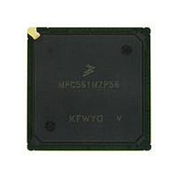
MPC561MZP56 Freescale, MPC561MZP56 Datasheet - Page 1318

MPC561MZP56
Manufacturer Part Number
MPC561MZP56
Description
Manufacturer
Freescale
Datasheet
1.MPC561MZP56.pdf
(1420 pages)
Specifications of MPC561MZP56
Cpu Family
MPC56x
Device Core
PowerPC
Device Core Size
32b
Frequency (max)
56MHz
Interface Type
QSPI/SCI/SPI/UART
Total Internal Ram Size
32KB
# I/os (max)
56
Number Of Timers - General Purpose
22
Operating Supply Voltage (typ)
2.6/5V
Operating Supply Voltage (max)
2.7/5.25V
Operating Supply Voltage (min)
2.5/4.75V
On-chip Adc
2(32-chx10-bit)
Instruction Set Architecture
RISC
Operating Temp Range
-40C to 125C
Operating Temperature Classification
Automotive
Mounting
Surface Mount
Pin Count
388
Package Type
BGA
Program Memory Type
ROMLess
Program Memory Size
Not Required
Lead Free Status / RoHS Status
Not Compliant
Available stocks
Company
Part Number
Manufacturer
Quantity
Price
Company:
Part Number:
MPC561MZP56
Manufacturer:
Freescale Semiconductor
Quantity:
10 000
Company:
Part Number:
MPC561MZP56R2
Manufacturer:
Freescale Semiconductor
Quantity:
10 000
- Current page: 1318 of 1420
- Download datasheet (11Mb)
66-MHz Electrical Characteristics
G.9
The supply symbols used in this section are described in
G-12
.
1
2
1
2
3
Array and CENSOR Data
These power supplies are only available on the MPC563 and MPC564.
Any supply in the V
“Keep-alive.”
A Program/Erase cycle is defined as switching the bits from 1 to 0 to 1.
A CENSOR Set/Clear cycle is defined as switching the bits from 1 to 0 to 1.
Maximum total time @ 150 °C junction temperature ≤ 1 year.
(High Voltage Supply Group)
CENSOR Set/Clear
(Low Voltage Supply Pins)
Array P/E Cycles
(Low Voltage Keep-Alive
Power-Up/Down Sequencing
Retention
Symbol
Cycles
Supply Pins
Symbol
V
V
V
DDKA
DDH
DDL
2
DDKA
1
2
group can be powered with the V
Maximum number of Program/Erase cycles per block to guarantee
data retention.
Minimum number of Program/Erase cycles per bit before failure.
Minimum data retention at an average of 85 °C junction temperature.
Minimum data retention at an average of 125 °C junction temperature.
MPC561/MPC563 Reference Manual, Rev. 1.2
Supply to the 5-V pads for output driver (V
Supply to the analog (QADC64E) circuitry (V
High voltage supply to the Flash module (V
Supply to low voltage pad drivers (QVDDL, NVDDL)
Supply to all low voltage internal logic (V
Supply to low voltage Flash circuitry (V
Supply to system PLL
Supply to IRAMSTBY
Supply to oscillator and other circuitry for keep-alive functions (KAPWR).
Table G-9. Power Supply Pin Groups
Table G-8. Flash Module Life
Meaning
DDL
if the function which it supplies is not required during
Table
Types of Power Pins
G-9.
DDF
DD
DDH
)
FLASH
)
1
DDA
)
)
)
1
Freescale Semiconductor
Min 15 years
Min 10 years
Value
1,000
100
3
3
Related parts for MPC561MZP56
Image
Part Number
Description
Manufacturer
Datasheet
Request
R

Part Number:
Description:
MPC5 1K0 5%
Manufacturer:
TE Connectivity
Datasheet:

Part Number:
Description:
MPC5 500R 5%
Manufacturer:
TE Connectivity
Datasheet:

Part Number:
Description:
MPC5 5K0 5%
Manufacturer:
Tyco Electronics
Datasheet:

Part Number:
Description:
MPC5 5R0 5%
Manufacturer:
Tyco Electronics
Datasheet:

Part Number:
Description:
MPC5 50K 5%
Manufacturer:
Tyco Electronics
Datasheet:

Part Number:
Description:
MPC5 1R0 5%
Manufacturer:
Tyco Electronics
Datasheet:

Part Number:
Description:
TOWER ELEVATOR BOARDS HARDWARE
Manufacturer:
Freescale Semiconductor
Datasheet:

Part Number:
Description:
TOWER SERIAL I/O HARDWARE
Manufacturer:
Freescale Semiconductor
Datasheet:

Part Number:
Description:
LCD MODULE FOR TWR SYSTEM
Manufacturer:
Freescale Semiconductor
Datasheet:

Part Number:
Description:
DAUGHTER LCD WVGA I.MX51
Manufacturer:
Freescale Semiconductor
Datasheet:

Part Number:
Description:
TOWER SYSTEM BOARD MPC5125
Manufacturer:
Freescale Semiconductor
Datasheet:


