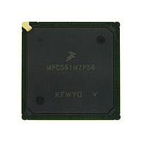
MPC561MZP56 Freescale, MPC561MZP56 Datasheet - Page 889

MPC561MZP56
Manufacturer Part Number
MPC561MZP56
Description
Manufacturer
Freescale
Datasheet
1.MPC561MZP56.pdf
(1420 pages)
Specifications of MPC561MZP56
Cpu Family
MPC56x
Device Core
PowerPC
Device Core Size
32b
Frequency (max)
56MHz
Interface Type
QSPI/SCI/SPI/UART
Total Internal Ram Size
32KB
# I/os (max)
56
Number Of Timers - General Purpose
22
Operating Supply Voltage (typ)
2.6/5V
Operating Supply Voltage (max)
2.7/5.25V
Operating Supply Voltage (min)
2.5/4.75V
On-chip Adc
2(32-chx10-bit)
Instruction Set Architecture
RISC
Operating Temp Range
-40C to 125C
Operating Temperature Classification
Automotive
Mounting
Surface Mount
Pin Count
388
Package Type
BGA
Program Memory Type
ROMLess
Program Memory Size
Not Required
Lead Free Status / RoHS Status
Not Compliant
Available stocks
Company
Part Number
Manufacturer
Quantity
Price
Company:
Part Number:
MPC561MZP56
Manufacturer:
Freescale Semiconductor
Quantity:
10 000
Company:
Part Number:
MPC561MZP56R2
Manufacturer:
Freescale Semiconductor
Quantity:
10 000
- Current page: 889 of 1420
- Download datasheet (11Mb)
Freescale Semiconductor
State
S1
S2
S3
S4
Normal Operation:
Normal array reads and register accesses. The
Block protect information can be modified.
Erase Hardware Interlock Write:
Normal read operation still occurs. The UC3F will
accept the erase hardware interlock write. This
write may be to any UC3F array location.
Accesses to the registers are normal register
accesses. A write to UC3FCTL cannot set EHV at
this time. A write to the register is not an erase
hardware interlock write and the UC3F remains in
state S2.
High voltage write enable
Accesses to the registers are normal register
accesses. A write to UC3FCTL can change SES
or EHV.
Erase Operation:
High voltage is applied to the array blocks to erase
the UC3F bit cells, and erase margin reads are
automatically performed by the embedded erase
control logic. During erase the array will not
respond to any address. Accesses to the registers
are allowed. A write to UC3FCTL can change EHV
or HSUS only.
Reset
Table 21-8. Erase Interlock State Descriptions
Mode
T1
MPC561/MPC563 Reference Manual, Rev. 1.2
Figure 21-10. Erase State Diagram
S2
S1
T2
T6
T3
T5
T10
T7
State
Next
S2
S1
S3
S1
S4
S1
S2
S5
S4
S3
T2
T1
T3
T6
T4
T5
T7
T8
T9
T4
Write PE = 1, SES = 1.
Write SES = 0 or a reset.
Hardware Interlock
A successful write to any UC3F array
location is the erase interlock write. If
the write is to a register the erase
hardware interlock write has not been
done and the UC3F remains in state
S2.
Write SES = 0 or a reset.
Write EHV = 1.
Reset.
Write EHV = 0.
Write HSUS = 1 or disable the UC3F
module.
Transition Requirement
T8
S5
CDR3 Flash (UC3F) EEPROM
21-27
Related parts for MPC561MZP56
Image
Part Number
Description
Manufacturer
Datasheet
Request
R

Part Number:
Description:
MPC5 1K0 5%
Manufacturer:
TE Connectivity
Datasheet:

Part Number:
Description:
MPC5 500R 5%
Manufacturer:
TE Connectivity
Datasheet:

Part Number:
Description:
MPC5 5K0 5%
Manufacturer:
Tyco Electronics
Datasheet:

Part Number:
Description:
MPC5 5R0 5%
Manufacturer:
Tyco Electronics
Datasheet:

Part Number:
Description:
MPC5 50K 5%
Manufacturer:
Tyco Electronics
Datasheet:

Part Number:
Description:
MPC5 1R0 5%
Manufacturer:
Tyco Electronics
Datasheet:

Part Number:
Description:
TOWER ELEVATOR BOARDS HARDWARE
Manufacturer:
Freescale Semiconductor
Datasheet:

Part Number:
Description:
TOWER SERIAL I/O HARDWARE
Manufacturer:
Freescale Semiconductor
Datasheet:

Part Number:
Description:
LCD MODULE FOR TWR SYSTEM
Manufacturer:
Freescale Semiconductor
Datasheet:

Part Number:
Description:
DAUGHTER LCD WVGA I.MX51
Manufacturer:
Freescale Semiconductor
Datasheet:

Part Number:
Description:
TOWER SYSTEM BOARD MPC5125
Manufacturer:
Freescale Semiconductor
Datasheet:


