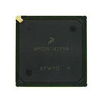
MPC561MZP56 Freescale, MPC561MZP56 Datasheet - Page 641

MPC561MZP56
Manufacturer Part Number
MPC561MZP56
Description
Manufacturer
Freescale
Datasheet
1.MPC561MZP56.pdf
(1420 pages)
Specifications of MPC561MZP56
Cpu Family
MPC56x
Device Core
PowerPC
Device Core Size
32b
Frequency (max)
56MHz
Interface Type
QSPI/SCI/SPI/UART
Total Internal Ram Size
32KB
# I/os (max)
56
Number Of Timers - General Purpose
22
Operating Supply Voltage (typ)
2.6/5V
Operating Supply Voltage (max)
2.7/5.25V
Operating Supply Voltage (min)
2.5/4.75V
On-chip Adc
2(32-chx10-bit)
Instruction Set Architecture
RISC
Operating Temp Range
-40C to 125C
Operating Temperature Classification
Automotive
Mounting
Surface Mount
Pin Count
388
Package Type
BGA
Program Memory Type
ROMLess
Program Memory Size
Not Required
Lead Free Status / RoHS Status
Not Compliant
Available stocks
Company
Part Number
Manufacturer
Quantity
Price
Company:
Part Number:
MPC561MZP56
Manufacturer:
Freescale Semiconductor
Quantity:
10 000
Company:
Part Number:
MPC561MZP56R2
Manufacturer:
Freescale Semiconductor
Quantity:
10 000
- Current page: 641 of 1420
- Download datasheet (11Mb)
15.6.2.1
Data received by the QSPI is stored in this segment, to be read by the CPU. Data stored in the receive RAM
is right-justified, (i.e., the least significant bit is always in the right-most bit position within the word
regardless of the serial transfer length). Unused bits in a receive queue entry are set to zero by the QSPI
upon completion of the individual queue entry. The CPU can access the data using byte, half-word, or word
addressing.
The CPTQP value in SPSR shows which queue entries have been executed. The CPU uses this information
to determine which locations in receive RAM contain valid data before reading them.
15.6.2.2
Data that is to be transmitted by the QSPI is stored in this segment. The CPU normally writes one word of
data into this segment for each queue command to be executed. If the corresponding peripheral, such as a
serial input port, is used solely to input data, then this segment does not need to be initialized.
Data must be written to transmit RAM in a right-justified format. The QSPI cannot modify information in
the transmit RAM. The QSPI copies the information to its data serializer for transmission. Information
remains in transmit RAM until overwritten.
15.6.2.3
Command RAM is used by the QSPI in master mode. The CPU writes one byte of control information to
this segment for each QSPI command to be executed. The QSPI cannot modify information in command
RAM.
Command RAM consists of 32 bytes. Each byte is divided into two fields. The peripheral chip-select field,
enables peripherals for transfer. The command control field provides transfer options.
A maximum of 32 commands can be in the queue. These bytes are assigned an address from 0x00 to 0x1F.
Queue execution by the QSPI proceeds from the address in NEWQP through the address in ENDQP. (Both
of these fields are in SPCR2.)
Freescale Semiconductor
or 0x30 5540
or 0x30 557F
0x30 5140
0x30 517F
Receive RAM
Transmit RAM
Command RAM
Half-Word
Receive
RAM
RRD
RRE
RRF
RR1
RR2
RR0
MPC561/MPC563 Reference Manual, Rev. 1.2
oe 0x30 55BF
or 0x30 5580
Figure 15-16. QSPI RAM
0x30 51BF
0x30 5180
Half-Word
Transmit
RAM
TRD
TRE
TR0
TR1
TR2
TRF
or 0x30 55DF
or 0x30 55C0
0x30 51DF
0x30 51C0
Queued Serial Multi-Channel Module
Command
RAM
CRD
CRE
CRF
CR0
CR1
CR2
Byte
15-23
Related parts for MPC561MZP56
Image
Part Number
Description
Manufacturer
Datasheet
Request
R

Part Number:
Description:
MPC5 1K0 5%
Manufacturer:
TE Connectivity
Datasheet:

Part Number:
Description:
MPC5 500R 5%
Manufacturer:
TE Connectivity
Datasheet:

Part Number:
Description:
MPC5 5K0 5%
Manufacturer:
Tyco Electronics
Datasheet:

Part Number:
Description:
MPC5 5R0 5%
Manufacturer:
Tyco Electronics
Datasheet:

Part Number:
Description:
MPC5 50K 5%
Manufacturer:
Tyco Electronics
Datasheet:

Part Number:
Description:
MPC5 1R0 5%
Manufacturer:
Tyco Electronics
Datasheet:

Part Number:
Description:
TOWER ELEVATOR BOARDS HARDWARE
Manufacturer:
Freescale Semiconductor
Datasheet:

Part Number:
Description:
TOWER SERIAL I/O HARDWARE
Manufacturer:
Freescale Semiconductor
Datasheet:

Part Number:
Description:
LCD MODULE FOR TWR SYSTEM
Manufacturer:
Freescale Semiconductor
Datasheet:

Part Number:
Description:
DAUGHTER LCD WVGA I.MX51
Manufacturer:
Freescale Semiconductor
Datasheet:

Part Number:
Description:
TOWER SYSTEM BOARD MPC5125
Manufacturer:
Freescale Semiconductor
Datasheet:


