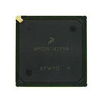
MPC561MZP56 Freescale, MPC561MZP56 Datasheet - Page 577

MPC561MZP56
Manufacturer Part Number
MPC561MZP56
Description
Manufacturer
Freescale
Datasheet
1.MPC561MZP56.pdf
(1420 pages)
Specifications of MPC561MZP56
Cpu Family
MPC56x
Device Core
PowerPC
Device Core Size
32b
Frequency (max)
56MHz
Interface Type
QSPI/SCI/SPI/UART
Total Internal Ram Size
32KB
# I/os (max)
56
Number Of Timers - General Purpose
22
Operating Supply Voltage (typ)
2.6/5V
Operating Supply Voltage (max)
2.7/5.25V
Operating Supply Voltage (min)
2.5/4.75V
On-chip Adc
2(32-chx10-bit)
Instruction Set Architecture
RISC
Operating Temp Range
-40C to 125C
Operating Temperature Classification
Automotive
Mounting
Surface Mount
Pin Count
388
Package Type
BGA
Program Memory Type
ROMLess
Program Memory Size
Not Required
Lead Free Status / RoHS Status
Not Compliant
Available stocks
Company
Part Number
Manufacturer
Quantity
Price
Company:
Part Number:
MPC561MZP56
Manufacturer:
Freescale Semiconductor
Quantity:
10 000
Company:
Part Number:
MPC561MZP56R2
Manufacturer:
Freescale Semiconductor
Quantity:
10 000
- Current page: 577 of 1420
- Download datasheet (11Mb)
The left justified, signed format corresponds to a half-scale, offset binary, two’s complement data format.
The data is routed onto the IMB3 according to the selected format. The address used to access the table
determines the data alignment format. All write operations to the result word table are right justified.
The three result data formats are produced by routing the RAM bits onto the data bus. The software
chooses among the three formats by reading the result at the memory address which produces the desired
data alignment.
The result word table is read/write accessible by software. During normal operation, applications software
only needs to read the result table. Write operations to the table may occur during test or debug breakpoint
operation. When locations in the CCW table are not used by an application, software could use the
corresponding locations in the result word table as scratch pad RAM, remembering that only 10 bits are
implemented. The result alignment is only implemented for software read operations. Since write
operations are not the normal use for the result registers, only one write data format is supported, which is
right justified data.
Freescale Semiconductor
1
SRESET
SRESET
SRESET
S = Sign bit.
Field
Addr
Field
Addr
Field
Addr
MSB
MSB
MSB
0
0
S
Some write operations, like bit manipulation, may not operate as expected
because the hardware cannot access a true 16-bit value.
0
1
1
1
1
Figure 14-17. Right Justified, Unsigned Result Format (RJURR)
Figure 14-19. Left Justified, Unsigned Result Register (LJURR)
Figure 14-18. Left Justified, Signed Result Format (LJSRR)
2
0000_00
2
2
—
3
3
0x30 4B80–4BFF (LJURR_A); 0x30 4F80–4FFF (LJURR_B)
0x30 4A80–4AFF (RJURR_A); 0x30 4E80–4EFF (RJURR_B)
3
0x30 4B00–4B7F (LJSRR_A); 0x30 4F00–4F7F (LJSRR_B)
MPC561/MPC563 Reference Manual, Rev. 1.2
Undefined
RESULT
Undefined
4
4
4
RESULT
5
5
5
6
6
6
NOTE
7
7
7
8
8
8
9
9
9
Undefined
10
10
10
RESULT
11
QADC64E Enhanced Mode Operation
11
11
12
00_0000
12
00_0000
12
—
—
13
13
13
14
14
14
LSB
LSB
15
LSB
15
15
14-35
Related parts for MPC561MZP56
Image
Part Number
Description
Manufacturer
Datasheet
Request
R

Part Number:
Description:
MPC5 1K0 5%
Manufacturer:
TE Connectivity
Datasheet:

Part Number:
Description:
MPC5 500R 5%
Manufacturer:
TE Connectivity
Datasheet:

Part Number:
Description:
MPC5 5K0 5%
Manufacturer:
Tyco Electronics
Datasheet:

Part Number:
Description:
MPC5 5R0 5%
Manufacturer:
Tyco Electronics
Datasheet:

Part Number:
Description:
MPC5 50K 5%
Manufacturer:
Tyco Electronics
Datasheet:

Part Number:
Description:
MPC5 1R0 5%
Manufacturer:
Tyco Electronics
Datasheet:

Part Number:
Description:
TOWER ELEVATOR BOARDS HARDWARE
Manufacturer:
Freescale Semiconductor
Datasheet:

Part Number:
Description:
TOWER SERIAL I/O HARDWARE
Manufacturer:
Freescale Semiconductor
Datasheet:

Part Number:
Description:
LCD MODULE FOR TWR SYSTEM
Manufacturer:
Freescale Semiconductor
Datasheet:

Part Number:
Description:
DAUGHTER LCD WVGA I.MX51
Manufacturer:
Freescale Semiconductor
Datasheet:

Part Number:
Description:
TOWER SYSTEM BOARD MPC5125
Manufacturer:
Freescale Semiconductor
Datasheet:


