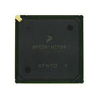
MPC561MZP56 Freescale, MPC561MZP56 Datasheet - Page 358

MPC561MZP56
Manufacturer Part Number
MPC561MZP56
Description
Manufacturer
Freescale
Datasheet
1.MPC561MZP56.pdf
(1420 pages)
Specifications of MPC561MZP56
Cpu Family
MPC56x
Device Core
PowerPC
Device Core Size
32b
Frequency (max)
56MHz
Interface Type
QSPI/SCI/SPI/UART
Total Internal Ram Size
32KB
# I/os (max)
56
Number Of Timers - General Purpose
22
Operating Supply Voltage (typ)
2.6/5V
Operating Supply Voltage (max)
2.7/5.25V
Operating Supply Voltage (min)
2.5/4.75V
On-chip Adc
2(32-chx10-bit)
Instruction Set Architecture
RISC
Operating Temp Range
-40C to 125C
Operating Temperature Classification
Automotive
Mounting
Surface Mount
Pin Count
388
Package Type
BGA
Program Memory Type
ROMLess
Program Memory Size
Not Required
Lead Free Status / RoHS Status
Not Compliant
Available stocks
Company
Part Number
Manufacturer
Quantity
Price
Company:
Part Number:
MPC561MZP56
Manufacturer:
Freescale Semiconductor
Quantity:
10 000
Company:
Part Number:
MPC561MZP56R2
Manufacturer:
Freescale Semiconductor
Quantity:
10 000
- Current page: 358 of 1420
- Download datasheet (11Mb)
External Bus Interface
The MPC561/MPC563 also supports burst-inhibited transfers for slave devices that are unable to support
bursting. For this type of bus cycle, the selected slave device supplies or samples the first word the
MPC561/MPC563 points to and asserts the burst-inhibit signal with TA for the first transfer of the burst
access. The MPC561/MPC563 responds by terminating the burst and accessing the remainder of the
16-byte block. These remaining accesses use up to three read/write bus cycles (each one for a word) in the
case of a 32-bit port width slave, up to seven read/write bus cycles in the case of a 16-bit port width slave,
or up to fifteen read/write bus cycles in the case of a 8-bit port width slave.
The general case of burst transfers assumes that the external memory has a 32-bit port size. The
MPC561/MPC563 provides an effective mechanism for interfacing with 16-bit and 8-bit port size
memories, allowing bursts transfers to these devices when they are controlled by the internal memory
controller.
In this case, the MPC561/MPC563 attempts to initiate a burst transfer as in the normal case. If the memory
controller signals to the bus interface that the external device has a small port size (8 or 16 bits), and if the
burst is accepted, the bus interface completes a burst of 16 or 8 beats respectively for four words. Eight
words requires 32 or 16 beats. Each beat of the burst transfers only one or two bytes effectively. Note that
this burst of 8 or 16 beats is considered an atomic transaction, so the MPC561/MPC563 does not allow
other unrelated master accesses or bus arbitration to intervene between the transfers.
9.5.5
In addition to the standard bus signals, the MPC561/MPC563 burst mechanism uses the following signals:
At the start of the burst transfer, the master drives the address, the address attributes, and the BURST signal
to indicate that a burst transfer is being initiated, and asserts TS. If the slave is burstable, it negates the
burst-inhibit (BI) signal. If the slave cannot burst, it asserts BI. For additional details, refer to
Section 10.2.5, “Burst
During the data phase of a burst-write cycle, the master drives the data. It also asserts BDIP if it intends to
drive the data beat following the current data beat. When the slave has received the data, it asserts TA to
indicate to the master that it is ready for the next data transfer. The master again drives the next data and
asserts or negates the BDIP signal. If the master does not intend to drive another data beat following the
current one, it negates BDIP to indicate to the slave that the next data beat transfer is the last data of the
burst-write transfer.
BDIP has two basic timings: normal and late (see
assertion of BDIP is delayed by the number of wait states in the first data beat. This implies that for
zero-wait-state cycles, BDIP assertion time is identical in normal and late modes. Cycles with late BDIP
generation can occur only during cycles for which the memory controller generates TA internally. Refer
to
9-18
Chapter 10, “Memory
•
•
•
The BURST signal indicates that the cycle is a burst cycle.
The burst data in progress (BDIP) signal indicates the duration of the burst data.
The burst inhibit (BI) signal indicates whether the slave is burstable.
Burst Mechanism
Support.”
Controller” for more information.
MPC561/MPC563 Reference Manual, Rev. 1.2
Figure 9-14
and
Figure
9-15). In the late timing mode,
Freescale Semiconductor
Related parts for MPC561MZP56
Image
Part Number
Description
Manufacturer
Datasheet
Request
R

Part Number:
Description:
MPC5 1K0 5%
Manufacturer:
TE Connectivity
Datasheet:

Part Number:
Description:
MPC5 500R 5%
Manufacturer:
TE Connectivity
Datasheet:

Part Number:
Description:
MPC5 5K0 5%
Manufacturer:
Tyco Electronics
Datasheet:

Part Number:
Description:
MPC5 5R0 5%
Manufacturer:
Tyco Electronics
Datasheet:

Part Number:
Description:
MPC5 50K 5%
Manufacturer:
Tyco Electronics
Datasheet:

Part Number:
Description:
MPC5 1R0 5%
Manufacturer:
Tyco Electronics
Datasheet:

Part Number:
Description:
TOWER ELEVATOR BOARDS HARDWARE
Manufacturer:
Freescale Semiconductor
Datasheet:

Part Number:
Description:
TOWER SERIAL I/O HARDWARE
Manufacturer:
Freescale Semiconductor
Datasheet:

Part Number:
Description:
LCD MODULE FOR TWR SYSTEM
Manufacturer:
Freescale Semiconductor
Datasheet:

Part Number:
Description:
DAUGHTER LCD WVGA I.MX51
Manufacturer:
Freescale Semiconductor
Datasheet:

Part Number:
Description:
TOWER SYSTEM BOARD MPC5125
Manufacturer:
Freescale Semiconductor
Datasheet:


