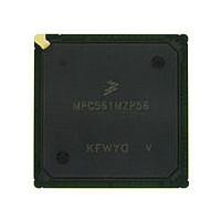
MPC561MZP56 Freescale, MPC561MZP56 Datasheet - Page 446

MPC561MZP56
Manufacturer Part Number
MPC561MZP56
Description
Manufacturer
Freescale
Datasheet
1.MPC561MZP56.pdf
(1420 pages)
Specifications of MPC561MZP56
Cpu Family
MPC56x
Device Core
PowerPC
Device Core Size
32b
Frequency (max)
56MHz
Interface Type
QSPI/SCI/SPI/UART
Total Internal Ram Size
32KB
# I/os (max)
56
Number Of Timers - General Purpose
22
Operating Supply Voltage (typ)
2.6/5V
Operating Supply Voltage (max)
2.7/5.25V
Operating Supply Voltage (min)
2.5/4.75V
On-chip Adc
2(32-chx10-bit)
Instruction Set Architecture
RISC
Operating Temp Range
-40C to 125C
Operating Temperature Classification
Automotive
Mounting
Surface Mount
Pin Count
388
Package Type
BGA
Program Memory Type
ROMLess
Program Memory Size
Not Required
Lead Free Status / RoHS Status
Not Compliant
Available stocks
Company
Part Number
Manufacturer
Quantity
Price
Company:
Part Number:
MPC561MZP56
Manufacturer:
Freescale Semiconductor
Quantity:
10 000
Company:
Part Number:
MPC561MZP56R2
Manufacturer:
Freescale Semiconductor
Quantity:
10 000
- Current page: 446 of 1420
- Download datasheet (11Mb)
L-Bus to U-Bus Interface (L2U)
11.7.1
L-bus show cycles are disabled during reset and must be configured by setting the LSHOW[0:1] bits in the
L2U_MCR.
11.7.2
When show cycles are enabled in the L2U module, there is a performance penalty on the L-bus. This
occurs because the L2U module does not support more than one access being processed at any time. To
ensure that only one access at a time is processed, and not lose an L-bus access that would have been show
cycled, the L2U module will arbitrate for the L-bus whenever it is processing any access. This L-bus
arbitration will prevent any other L-bus master from starting a cycle that might turn out to be a qualifiable
L-bus show cycle.
For L-bus show cycles, the minimum performance impact on the L-bus will be three clocks. This minimum
impact assumes that the L-bus slave access is a 1-clock access, and the L2U module acquires immediate
bus grant on the U-bus. The L2U has to wait two clocks before completing the show cycle on the U-Bus,
thus using up five clocks for the complete process.
A retried access on the L-bus (no address acknowledge) that qualifies to be show cycled, will be accepted
when it is actually acknowledged. This will cause a 1-clock delay before an L-bus master can retry the
access on the L-bus, because the L2U module will release L-bus one clock later.
L2U asserts the internal bus request signal on the U-bus for a minimum of two clocks when starting a show
cycle on the U-bus.
11.7.3
The L2U module behaves as both a master and a slave on the U-bus during show cycles. The L2U starts
the U-bus transfer as a bus master and then completes the address phase and data phase of the cycle as a
slave. The L2U follows U-bus protocol of in-order termination of the data phase.
The USIU can control the start of show cycles on the U-bus by asserting the no-show cycle indicator. This
will cause the L2U module to release the U-bus for at least one clock before retrying the show cycle.
11.7.4
The L2U performs the following sequence of actions for an L-bus-write show cycle.
11-10
1. Arbitrates for the L-bus to prevent any other L-bus cycles from starting
Programming Show Cycles
Performance Impact
Show Cycle Protocol
L-Bus Write Show Cycle Flow
Table 11-3
LSHOW
00
01
10
11
shows the configurations of the LSHOW[0:1] bits.
MPC561/MPC563 Reference Manual, Rev. 1.2
Show address and data of all L-bus space read and write cycles
Table 11-3. L2U_MCR LSHOW Modes
Show address and data of all L-bus space write cycles
Reserved (Disable L-bus show cycles)
Disable L-bus show cycles
Action
Freescale Semiconductor
Related parts for MPC561MZP56
Image
Part Number
Description
Manufacturer
Datasheet
Request
R

Part Number:
Description:
MPC5 1K0 5%
Manufacturer:
TE Connectivity
Datasheet:

Part Number:
Description:
MPC5 500R 5%
Manufacturer:
TE Connectivity
Datasheet:

Part Number:
Description:
MPC5 5K0 5%
Manufacturer:
Tyco Electronics
Datasheet:

Part Number:
Description:
MPC5 5R0 5%
Manufacturer:
Tyco Electronics
Datasheet:

Part Number:
Description:
MPC5 50K 5%
Manufacturer:
Tyco Electronics
Datasheet:

Part Number:
Description:
MPC5 1R0 5%
Manufacturer:
Tyco Electronics
Datasheet:

Part Number:
Description:
TOWER ELEVATOR BOARDS HARDWARE
Manufacturer:
Freescale Semiconductor
Datasheet:

Part Number:
Description:
TOWER SERIAL I/O HARDWARE
Manufacturer:
Freescale Semiconductor
Datasheet:

Part Number:
Description:
LCD MODULE FOR TWR SYSTEM
Manufacturer:
Freescale Semiconductor
Datasheet:

Part Number:
Description:
DAUGHTER LCD WVGA I.MX51
Manufacturer:
Freescale Semiconductor
Datasheet:

Part Number:
Description:
TOWER SYSTEM BOARD MPC5125
Manufacturer:
Freescale Semiconductor
Datasheet:


