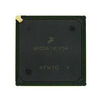
MPC561MZP56 Freescale, MPC561MZP56 Datasheet - Page 432

MPC561MZP56
Manufacturer Part Number
MPC561MZP56
Description
Manufacturer
Freescale
Datasheet
1.MPC561MZP56.pdf
(1420 pages)
Specifications of MPC561MZP56
Cpu Family
MPC56x
Device Core
PowerPC
Device Core Size
32b
Frequency (max)
56MHz
Interface Type
QSPI/SCI/SPI/UART
Total Internal Ram Size
32KB
# I/os (max)
56
Number Of Timers - General Purpose
22
Operating Supply Voltage (typ)
2.6/5V
Operating Supply Voltage (max)
2.7/5.25V
Operating Supply Voltage (min)
2.5/4.75V
On-chip Adc
2(32-chx10-bit)
Instruction Set Architecture
RISC
Operating Temp Range
-40C to 125C
Operating Temperature Classification
Automotive
Mounting
Surface Mount
Pin Count
388
Package Type
BGA
Program Memory Type
ROMLess
Program Memory Size
Not Required
Lead Free Status / RoHS Status
Not Compliant
Available stocks
Company
Part Number
Manufacturer
Quantity
Price
Company:
Part Number:
MPC561MZP56
Manufacturer:
Freescale Semiconductor
Quantity:
10 000
Company:
Part Number:
MPC561MZP56R2
Manufacturer:
Freescale Semiconductor
Quantity:
10 000
- Current page: 432 of 1420
- Download datasheet (11Mb)
Memory Controller
10.9.4
10-34
1,
Bits
30
31
1
It is recommended that this field hold values that are the power of 2 minus 1 (e.g., 2
HRESET
HRESET
Memory Controller Option Registers (OR0–OR3)
Field
Addr
Name
BI
V
MSB
AM
16
0
Burst inhibit
0 Memory controller drives BI negated (high). The bank supports burst accesses.
1 Memory controller drives BI asserted (low). The bank does not support burst accesses.
NOTE: Following a system reset, the BI bit is set.
Valid bit. When set, this bit indicates that the contents of the base-register and option-register
pair are valid. The CS signal does not assert until the V-bit is set.
NOTE: An access to a region that has no V-bit set may cause a bus monitor timeout. See
Table 10-9
Figure 10-24. Memory Controller Option Registers 1–3 (OR0–OR3)
17
1
Branch Register
0x2F C104 (OR0); 0x2F C10C (OR1); 0x2F C114 (OR2), 0x2F C11C (OR3)
Table 10-8. BR0–BR3 Bit Descriptions (continued)
ATM
18
2
BR0
BR1
BR2
BR3
for the reset value of this bit in BR0.
MPC561/MPC563 Reference Manual, Rev. 1.2
19
3
0000_0000
Table 10-9. BRx[V] Reset Value
CSNT
20
4
21
5
ACS
0000_0000_0000_0000
22
6
EHTR
23
7
Description
AM
1
24
8
BRx[V] Reset Value
25
ID20 & ID31
9
1111
SCY
ID3
10
26
0
0
11
27
3
- 1 = 7 [0b111]).
12
28
0
BSCY
Freescale Semiconductor
13
29
1
14
30
1
TRLX
LSB
15
31
0
Related parts for MPC561MZP56
Image
Part Number
Description
Manufacturer
Datasheet
Request
R

Part Number:
Description:
MPC5 1K0 5%
Manufacturer:
TE Connectivity
Datasheet:

Part Number:
Description:
MPC5 500R 5%
Manufacturer:
TE Connectivity
Datasheet:

Part Number:
Description:
MPC5 5K0 5%
Manufacturer:
Tyco Electronics
Datasheet:

Part Number:
Description:
MPC5 5R0 5%
Manufacturer:
Tyco Electronics
Datasheet:

Part Number:
Description:
MPC5 50K 5%
Manufacturer:
Tyco Electronics
Datasheet:

Part Number:
Description:
MPC5 1R0 5%
Manufacturer:
Tyco Electronics
Datasheet:

Part Number:
Description:
TOWER ELEVATOR BOARDS HARDWARE
Manufacturer:
Freescale Semiconductor
Datasheet:

Part Number:
Description:
TOWER SERIAL I/O HARDWARE
Manufacturer:
Freescale Semiconductor
Datasheet:

Part Number:
Description:
LCD MODULE FOR TWR SYSTEM
Manufacturer:
Freescale Semiconductor
Datasheet:

Part Number:
Description:
DAUGHTER LCD WVGA I.MX51
Manufacturer:
Freescale Semiconductor
Datasheet:

Part Number:
Description:
TOWER SYSTEM BOARD MPC5125
Manufacturer:
Freescale Semiconductor
Datasheet:


