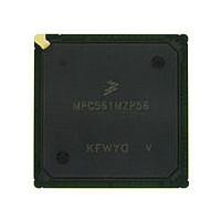
MPC561MZP56 Freescale, MPC561MZP56 Datasheet - Page 433

MPC561MZP56
Manufacturer Part Number
MPC561MZP56
Description
Manufacturer
Freescale
Datasheet
1.MPC561MZP56.pdf
(1420 pages)
Specifications of MPC561MZP56
Cpu Family
MPC56x
Device Core
PowerPC
Device Core Size
32b
Frequency (max)
56MHz
Interface Type
QSPI/SCI/SPI/UART
Total Internal Ram Size
32KB
# I/os (max)
56
Number Of Timers - General Purpose
22
Operating Supply Voltage (typ)
2.6/5V
Operating Supply Voltage (max)
2.7/5.25V
Operating Supply Voltage (min)
2.5/4.75V
On-chip Adc
2(32-chx10-bit)
Instruction Set Architecture
RISC
Operating Temp Range
-40C to 125C
Operating Temperature Classification
Automotive
Mounting
Surface Mount
Pin Count
388
Package Type
BGA
Program Memory Type
ROMLess
Program Memory Size
Not Required
Lead Free Status / RoHS Status
Not Compliant
Available stocks
Company
Part Number
Manufacturer
Quantity
Price
Company:
Part Number:
MPC561MZP56
Manufacturer:
Freescale Semiconductor
Quantity:
10 000
Company:
Part Number:
MPC561MZP56R2
Manufacturer:
Freescale Semiconductor
Quantity:
10 000
- Current page: 433 of 1420
- Download datasheet (11Mb)
Freescale Semiconductor
17:19
21:22
24:27
Bits
0:16
20
23
Name
CSNT
EHTR
ATM
ACS
SCY
AM
Address mask. This field allows masking of any corresponding bits in the associated base
register. Masking the address bits independently allows external devices of different size address
ranges to be used. Any clear bit masks the corresponding address bit. Any set bit causes the
corresponding address bit to be used in comparison with the address signals. Address mask bits
can be set or cleared in any order in the field, allowing a resource to reside in more than one area
of the address map. This field can be read or written at anytime.
Following a system reset, the AM bits are cleared in OR0.
Address type mask. This field masks selected address type bits, allowing more than one address
space type to be assigned to a chip-select. Any set bit causes the corresponding address type
code bits to be used as part of the address comparison. Any cleared bit masks the corresponding
address type code bit. Clear the ATM bits to ignore address type codes as part of the address
comparison. Note that the address type field uses only AT[0:2] and does not need AT3 to define
the memory type space.
Following a system reset, the ATM bits are cleared in OR0.
Chip-select negation time. Following a system reset, the CSNT bit is reset in OR0.
0 CS/WE are negated normally.
1 CS/WE are negated a quarter of a clock earlier than normal
Following a system reset, the CSNT bit is cleared in OR0.
Address to chip-select setup. Following a system reset, the ACS bits are reset in OR0.
00 CS is asserted at the same time that the address lines are valid.
01 Reserved
10 CS is asserted a quarter of a clock after the address lines are valid.
11 CS is asserted half a clock after the address lines are valid
Following a system reset, the ACS bits are cleared in OR0.
Extended hold time on read accesses. This bit, when asserted, inserts an idle clock cycle after
a read access from the current bank and any MPC561/MPC563 write accesses or read accesses
to a different bank.
0 Memory controller generates normal timing
1 Memory controller generates extended hold timing
Following a system reset, the EHTR bits are cleared in OR0.
Cycle length in clocks. This four-bit value represents the number of wait states inserted in the
single cycle, or in the first beat of a burst, when the GPCM handles the external memory access.
Values range from 0 (0b0000) to 15 (0b1111). This is the main parameter for determining the
length of the cycle.
The total cycle length may vary depending on the settings of other timing attributes.
The total memory access length is (2 + SCY) x Clocks.
If an external TA response is selected for this memory bank (by setting the SETA bit), then the
SCY field is not used.
Following a system reset, the SCY bits are set to 0b1111 in OR0.
MPC561/MPC563 Reference Manual, Rev. 1.2
Table 10-10. OR0–OR3 Bit Descriptions
Description
Memory Controller
10-35
Related parts for MPC561MZP56
Image
Part Number
Description
Manufacturer
Datasheet
Request
R

Part Number:
Description:
MPC5 1K0 5%
Manufacturer:
TE Connectivity
Datasheet:

Part Number:
Description:
MPC5 500R 5%
Manufacturer:
TE Connectivity
Datasheet:

Part Number:
Description:
MPC5 5K0 5%
Manufacturer:
Tyco Electronics
Datasheet:

Part Number:
Description:
MPC5 5R0 5%
Manufacturer:
Tyco Electronics
Datasheet:

Part Number:
Description:
MPC5 50K 5%
Manufacturer:
Tyco Electronics
Datasheet:

Part Number:
Description:
MPC5 1R0 5%
Manufacturer:
Tyco Electronics
Datasheet:

Part Number:
Description:
TOWER ELEVATOR BOARDS HARDWARE
Manufacturer:
Freescale Semiconductor
Datasheet:

Part Number:
Description:
TOWER SERIAL I/O HARDWARE
Manufacturer:
Freescale Semiconductor
Datasheet:

Part Number:
Description:
LCD MODULE FOR TWR SYSTEM
Manufacturer:
Freescale Semiconductor
Datasheet:

Part Number:
Description:
DAUGHTER LCD WVGA I.MX51
Manufacturer:
Freescale Semiconductor
Datasheet:

Part Number:
Description:
TOWER SYSTEM BOARD MPC5125
Manufacturer:
Freescale Semiconductor
Datasheet:


