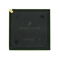
MPC561MZP56 Freescale, MPC561MZP56 Datasheet - Page 306

MPC561MZP56
Manufacturer Part Number
MPC561MZP56
Description
Manufacturer
Freescale
Datasheet
1.MPC561MZP56.pdf
(1420 pages)
Specifications of MPC561MZP56
Cpu Family
MPC56x
Device Core
PowerPC
Device Core Size
32b
Frequency (max)
56MHz
Interface Type
QSPI/SCI/SPI/UART
Total Internal Ram Size
32KB
# I/os (max)
56
Number Of Timers - General Purpose
22
Operating Supply Voltage (typ)
2.6/5V
Operating Supply Voltage (max)
2.7/5.25V
Operating Supply Voltage (min)
2.5/4.75V
On-chip Adc
2(32-chx10-bit)
Instruction Set Architecture
RISC
Operating Temp Range
-40C to 125C
Operating Temperature Classification
Automotive
Mounting
Surface Mount
Pin Count
388
Package Type
BGA
Program Memory Type
ROMLess
Program Memory Size
Not Required
Lead Free Status / RoHS Status
Not Compliant
Available stocks
Company
Part Number
Manufacturer
Quantity
Price
Company:
Part Number:
MPC561MZP56
Manufacturer:
Freescale Semiconductor
Quantity:
10 000
Company:
Part Number:
MPC561MZP56R2
Manufacturer:
Freescale Semiconductor
Quantity:
10 000
- Current page: 306 of 1420
- Download datasheet (11Mb)
Clocks and Power Control
8.2.1
The PLL can multiply the input frequency by any integer between one and 4096. The multiplication factor
depends on the value of the MF[0:11] bits in the PLPRCR register. While any integer value from one to
4096 can be programmed, the resulting VCO output frequency must be at least 15 MHz. The multiplication
factor is set to a predetermined value during power-on reset as defined in
8.2.2
The PLL is capable of eliminating the skew between the external clock entering the chip (EXTCLK) and
both the internal clock phases and the CLKOUT pin, making it useful for tight synchronous timings. Skew
elimination is active only when the PLL is enabled and programmed with a multiplication factor of one or
two (MF = 0 or 1). The timing reference to the system PLL is the external clock input (EXTCLK pin).
8.2.3
A pre-divider before the phase comparator enables additional system clock resolution when the crystal
oscillator frequency is 20 MHz. The division factor is determined by the DIVF[0:4] bits in the PLPRCR.
8.2.4
As shown in
comparator controls the direction (up or down) that the charge pump drives the voltage across the external
filter capacitor (XFC). The direction depends on whether the feedback signal phase lags or leads the
reference signal. The output of the charge pump drives the VCO. The output frequency of the VCO is
divided down and fed back to the phase comparator for comparison with the reference signal, OSCCLK.
The MF values, zero to 4095, are mapped to multiplication factors of one to 4096. Note that when the PLL
is operating in 1:1 mode (refer to
frequency is twice the maximum system frequency. This double frequency is needed to generate GCLK1
and GCLK2 clocks. On power-up, with a 4-MHz or 20-MHz crystal and the default MF settings,
VCOOUT will be 40 MHz and the system clock will be 20 MHz.
The equation for VCOOUT is:
In the case of initial system power up, or if KAPWR is lost, an external circuit must assert power on reset
(PORESET). Once KAPWR is valid, PORESET must be asserted long enough to allow the external
oscillator to start up and stabilize for the device to come out of reset in normal (non limp) mode.
8-4
Frequency Multiplication
Skew Elimination
Pre-Divider
PLL Block Diagram
Figure
When operating with the backup clock, the system clock (and CLKOUT) is
one-half of the ring oscillator frequency, (i.e., the system clock is
approximately 11 MHz). The time base and PIT clocks will be twice the
system clock frequency.
8-3, the reference signal, OSCCLK, goes to the phase comparator. The phase
VCOOUT =
MPC561/MPC563 Reference Manual, Rev. 1.2
Table
8-1), the multiplication factor is one (MF = 0). The PLL output
OSCCLK
DIVF + 1
NOTE
x (MF + 1) x 2
Table
8-1.
Freescale Semiconductor
Related parts for MPC561MZP56
Image
Part Number
Description
Manufacturer
Datasheet
Request
R

Part Number:
Description:
MPC5 1K0 5%
Manufacturer:
TE Connectivity
Datasheet:

Part Number:
Description:
MPC5 500R 5%
Manufacturer:
TE Connectivity
Datasheet:

Part Number:
Description:
MPC5 5K0 5%
Manufacturer:
Tyco Electronics
Datasheet:

Part Number:
Description:
MPC5 5R0 5%
Manufacturer:
Tyco Electronics
Datasheet:

Part Number:
Description:
MPC5 50K 5%
Manufacturer:
Tyco Electronics
Datasheet:

Part Number:
Description:
MPC5 1R0 5%
Manufacturer:
Tyco Electronics
Datasheet:

Part Number:
Description:
TOWER ELEVATOR BOARDS HARDWARE
Manufacturer:
Freescale Semiconductor
Datasheet:

Part Number:
Description:
TOWER SERIAL I/O HARDWARE
Manufacturer:
Freescale Semiconductor
Datasheet:

Part Number:
Description:
LCD MODULE FOR TWR SYSTEM
Manufacturer:
Freescale Semiconductor
Datasheet:

Part Number:
Description:
DAUGHTER LCD WVGA I.MX51
Manufacturer:
Freescale Semiconductor
Datasheet:

Part Number:
Description:
TOWER SYSTEM BOARD MPC5125
Manufacturer:
Freescale Semiconductor
Datasheet:


