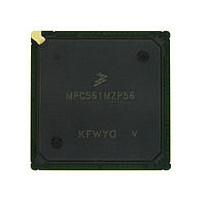
MPC561MZP56 Freescale, MPC561MZP56 Datasheet - Page 307

MPC561MZP56
Manufacturer Part Number
MPC561MZP56
Description
Manufacturer
Freescale
Datasheet
1.MPC561MZP56.pdf
(1420 pages)
Specifications of MPC561MZP56
Cpu Family
MPC56x
Device Core
PowerPC
Device Core Size
32b
Frequency (max)
56MHz
Interface Type
QSPI/SCI/SPI/UART
Total Internal Ram Size
32KB
# I/os (max)
56
Number Of Timers - General Purpose
22
Operating Supply Voltage (typ)
2.6/5V
Operating Supply Voltage (max)
2.7/5.25V
Operating Supply Voltage (min)
2.5/4.75V
On-chip Adc
2(32-chx10-bit)
Instruction Set Architecture
RISC
Operating Temp Range
-40C to 125C
Operating Temperature Classification
Automotive
Mounting
Surface Mount
Pin Count
388
Package Type
BGA
Program Memory Type
ROMLess
Program Memory Size
Not Required
Lead Free Status / RoHS Status
Not Compliant
Available stocks
Company
Part Number
Manufacturer
Quantity
Price
Company:
Part Number:
MPC561MZP56
Manufacturer:
Freescale Semiconductor
Quantity:
10 000
Company:
Part Number:
MPC561MZP56R2
Manufacturer:
Freescale Semiconductor
Quantity:
10 000
- Current page: 307 of 1420
- Download datasheet (11Mb)
If limp mode is enabled (by the MODCK[1:3] pins), and PORESET is negated before the external
oscillator has started up, the backup clock, BUCLK, will be used to clock the device. The device will start
to run in limp mode. Software can then switch the clock mode from BUCLK to PLL. If an application
requires that the device always comes out of reset in normal mode, PORESET should be asserted long
enough for the external oscillator to start up. The maximum start-up time of an external oscillator is given
in
additional 100, 000 input clock cycles.
If limp mode is disabled at reset, a short reset of at least 3 µs is enough to obtain normal chip operation,
because the BUCLK will not start. The system will wait for the external oscillator to start-up and stabilize.
The PLL will begin to lock once PORESET has been negated, assuming stable KAPWR and VDDSYN
power supplies and internal oscillator (or external clock). The PLL maximum lock time is determined by
the input clock to the phase comparator. The PLL locks within 500 input clock cycles if the PLPRCR[MF]
<= 4. The PLL locks within 1000 input clock cycles if PLPRCR[MF] >4. HRESET will be released 512
system clock cycles after the PLL locks.
Whenever PORESET is asserted, the MF bits are set according to
frequency (DFNH) and division factor low frequency (DFNL) bits in SCCR are set to the value of 0 (÷1
for DFNH and ÷2 for DFNL).
8.2.5
The following pins are dedicated to the PLL operation:
Freescale Semiconductor
Appendix F, “Electrical
•
•
OSCCLK
VDDSYN — Drain voltage. This is the V
should be well-regulated and the pin should be provided with an extremely low impedance path to
the V
close as possible to the chip package.
VSSSYN — Source voltage. This is the V
be provided with an extremely low impedance path to ground. VSSSYN should be bypassed to
VDDSYN by a 0.1 µF capacitor located as close as possible to the chip package.
PLL Pins
DD
Division Factor
power rail. VDDSYN should be bypassed to VSSSYN by a 0.1 µF capacitor located as
DIVF[0:4]
Feedback
Characteristics” and PORESET should be asserted for this time and at least an
MPC561/MPC563 Reference Manual, Rev. 1.2
Figure 8-3. System PLL Block Diagram
Comparator
Phase
Delay
Clock
Down
Up
DD
SS
dedicated to the analog PLL circuits. The pin should
dedicated to the analog PLL circuits. The voltage
Charge
Pump
Table
Multiplication Factor
XFC
MF[0:11]
8-1, and the division factor high
VCO
Clocks and Power Control
VCOOUT
VDDSYN
VSSSYN
8-5
Related parts for MPC561MZP56
Image
Part Number
Description
Manufacturer
Datasheet
Request
R

Part Number:
Description:
MPC5 1K0 5%
Manufacturer:
TE Connectivity
Datasheet:

Part Number:
Description:
MPC5 500R 5%
Manufacturer:
TE Connectivity
Datasheet:

Part Number:
Description:
MPC5 5K0 5%
Manufacturer:
Tyco Electronics
Datasheet:

Part Number:
Description:
MPC5 5R0 5%
Manufacturer:
Tyco Electronics
Datasheet:

Part Number:
Description:
MPC5 50K 5%
Manufacturer:
Tyco Electronics
Datasheet:

Part Number:
Description:
MPC5 1R0 5%
Manufacturer:
Tyco Electronics
Datasheet:

Part Number:
Description:
TOWER ELEVATOR BOARDS HARDWARE
Manufacturer:
Freescale Semiconductor
Datasheet:

Part Number:
Description:
TOWER SERIAL I/O HARDWARE
Manufacturer:
Freescale Semiconductor
Datasheet:

Part Number:
Description:
LCD MODULE FOR TWR SYSTEM
Manufacturer:
Freescale Semiconductor
Datasheet:

Part Number:
Description:
DAUGHTER LCD WVGA I.MX51
Manufacturer:
Freescale Semiconductor
Datasheet:

Part Number:
Description:
TOWER SYSTEM BOARD MPC5125
Manufacturer:
Freescale Semiconductor
Datasheet:


