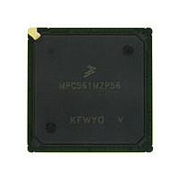
MPC561MZP56 Freescale, MPC561MZP56 Datasheet - Page 979

MPC561MZP56
Manufacturer Part Number
MPC561MZP56
Description
Manufacturer
Freescale
Datasheet
1.MPC561MZP56.pdf
(1420 pages)
Specifications of MPC561MZP56
Cpu Family
MPC56x
Device Core
PowerPC
Device Core Size
32b
Frequency (max)
56MHz
Interface Type
QSPI/SCI/SPI/UART
Total Internal Ram Size
32KB
# I/os (max)
56
Number Of Timers - General Purpose
22
Operating Supply Voltage (typ)
2.6/5V
Operating Supply Voltage (max)
2.7/5.25V
Operating Supply Voltage (min)
2.5/4.75V
On-chip Adc
2(32-chx10-bit)
Instruction Set Architecture
RISC
Operating Temp Range
-40C to 125C
Operating Temperature Classification
Automotive
Mounting
Surface Mount
Pin Count
388
Package Type
BGA
Program Memory Type
ROMLess
Program Memory Size
Not Required
Lead Free Status / RoHS Status
Not Compliant
Available stocks
Company
Part Number
Manufacturer
Quantity
Price
Company:
Part Number:
MPC561MZP56
Manufacturer:
Freescale Semiconductor
Quantity:
10 000
Company:
Part Number:
MPC561MZP56R2
Manufacturer:
Freescale Semiconductor
Quantity:
10 000
- Current page: 979 of 1420
- Download datasheet (11Mb)
Table 24-8
24.6.1.5
The MC register is used to select different modes of the READI module.
register bits.
Freescale Semiconductor
1
RCPU
Bits
The DOR and DME fields in the DC register can only be modified when system reset is asserted, or reset (to default
state) when the READI module is reset by the assertion of RSTI.
3:5
6:7
0
1
2
describes the DC register fields with the mode configurations for RCPU development access.
Nexus
Mode Control Register (MC)
Bits
DOR
4:2
1:0
7
6
5
0
1
x
Name
DOR
DME
DPA
TM
EC
DME
1
1
0
1
1
Table 24-8. RCPU Development Access Modes
READI Debug Mode Entry Out-of-reset Field can be configured to enable or disable
debug mode entry out of reset.
0 Debug Mode Not Entered Out-of-Reset
1 Debug Mode Entered Out-of-Reset
READI Debug Mode Enable Field can be configured to enable or disable debug
mode.
0 Debug Mode Disabled
1 Debug Mode Enabled
Reserved
READI Trace Mode Field can be configured to enable BTM, DTM, and OTM. Any or
all types of trace may be enabled.
000 No Trace
1xx BTM Branch Trace Messaging Enabled
x1x DTM Data Trace Messaging Enabled
xx1 OTM Ownership Trace Messaging Enabled
READI EVTI Control Field can be configured for synchronization and breakpoint
generation. If the EC is equal to 0b00, asserting EVTI will cause the next program and
data trace message to be a synchronization message (providing program and data
trace are enabled). If the EC field is equal to 0b01, a breakpoint will be generated. If
the field is configured to one of the reserved states, its action reverts to that of the
default state.
NOTE: The EVTI signal is level sensitive when EC is configured for breakpoint
generation. This implies that as long as EVTI assertion is continued (with EC set to
0b01), the READI module will continue requesting a breakpoint. The user must detect
breakpoint generation and negate the EVTI signal appropriately.
00 EVTI for program and data trace synchronization
01 EVTI for breakpoint generation
1x No Action
MPC561/MPC563 Reference Manual, Rev. 1.2
Non-debug mode access of RCPU development through READI.
Debug mode is enabled through READI (RCPU is still in normal mode, out
of reset)
Debug mode is enabled through READI and entered out-of-reset. Debug
mode entry causes RCPU to halt.
Table 24-7. DC Bit Descriptions
RCPU Development Access through READI
Description
Table 24-7
shows the location of
READI Module
24-11
Related parts for MPC561MZP56
Image
Part Number
Description
Manufacturer
Datasheet
Request
R

Part Number:
Description:
MPC5 1K0 5%
Manufacturer:
TE Connectivity
Datasheet:

Part Number:
Description:
MPC5 500R 5%
Manufacturer:
TE Connectivity
Datasheet:

Part Number:
Description:
MPC5 5K0 5%
Manufacturer:
Tyco Electronics
Datasheet:

Part Number:
Description:
MPC5 5R0 5%
Manufacturer:
Tyco Electronics
Datasheet:

Part Number:
Description:
MPC5 50K 5%
Manufacturer:
Tyco Electronics
Datasheet:

Part Number:
Description:
MPC5 1R0 5%
Manufacturer:
Tyco Electronics
Datasheet:

Part Number:
Description:
TOWER ELEVATOR BOARDS HARDWARE
Manufacturer:
Freescale Semiconductor
Datasheet:

Part Number:
Description:
TOWER SERIAL I/O HARDWARE
Manufacturer:
Freescale Semiconductor
Datasheet:

Part Number:
Description:
LCD MODULE FOR TWR SYSTEM
Manufacturer:
Freescale Semiconductor
Datasheet:

Part Number:
Description:
DAUGHTER LCD WVGA I.MX51
Manufacturer:
Freescale Semiconductor
Datasheet:

Part Number:
Description:
TOWER SYSTEM BOARD MPC5125
Manufacturer:
Freescale Semiconductor
Datasheet:


