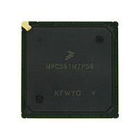
MPC561MZP56 Freescale, MPC561MZP56 Datasheet - Page 549

MPC561MZP56
Manufacturer Part Number
MPC561MZP56
Description
Manufacturer
Freescale
Datasheet
1.MPC561MZP56.pdf
(1420 pages)
Specifications of MPC561MZP56
Cpu Family
MPC56x
Device Core
PowerPC
Device Core Size
32b
Frequency (max)
56MHz
Interface Type
QSPI/SCI/SPI/UART
Total Internal Ram Size
32KB
# I/os (max)
56
Number Of Timers - General Purpose
22
Operating Supply Voltage (typ)
2.6/5V
Operating Supply Voltage (max)
2.7/5.25V
Operating Supply Voltage (min)
2.5/4.75V
On-chip Adc
2(32-chx10-bit)
Instruction Set Architecture
RISC
Operating Temp Range
-40C to 125C
Operating Temperature Classification
Automotive
Mounting
Surface Mount
Pin Count
388
Package Type
BGA
Program Memory Type
ROMLess
Program Memory Size
Not Required
Lead Free Status / RoHS Status
Not Compliant
Available stocks
Company
Part Number
Manufacturer
Quantity
Price
Company:
Part Number:
MPC561MZP56
Manufacturer:
Freescale Semiconductor
Quantity:
10 000
Company:
Part Number:
MPC561MZP56R2
Manufacturer:
Freescale Semiconductor
Quantity:
10 000
- Current page: 549 of 1420
- Download datasheet (11Mb)
Table 14-4
multiplexer chips using one QADC module.
14.3
The QADC64E has three global registers for configuring module operation.
These global registers are always defined to be in supervisor-only data space. Refer to
QADC64E_A Address Map and
“Supervisor/Unrestricted Address
The remaining five registers in the control register block control the operation of the queuing mechanism,
and provide a means of monitoring the operation of the QADC64E.
The Conversion Command Word (CCW) table contains 64 entries to hold the software programmable
analog conversion sequences. Each CCW table entry is a 16-bit entry, though only 10 bits are used.
The final block of address space belongs to the result word table, which appears in three places in the
memory map. Each result word table location holds one 10-bit conversion value.
Freescale Semiconductor
•
•
•
•
•
•
•
The module configuration register, QADCMCR
Configuration
The interrupt register, QADCINT
The test register, QADCTEST. This register is used for factory test only.
Control register 0 (QACR0) contains hardware configuration information
“Control Register
Control register 1 (QACR1) is associated with queue 1
Control register 2 (QACR2) is associated with queue 2
Status registers (QASR0 and QASR1) provide visibility on the status of each queue and the
particular conversion that is in progress
Programming the QADC64E Registers
shows the total number of analog input channels supported with zero to four external
No External
If a QADC64E module is in external multiplexing (EMUX) mode then the
multiplexer address signal channels AN[52:54] should not be programmed
into queues.
MUX Chips
16
Register”)
0”)
Directly Connected + External Multiplexed = Total Channels
NOTE: QADC64E External MUX Users
One External
MUX Chip
MPC561/MPC563 Reference Manual, Rev. 1.2
Number of Analog Input Channels Available
Table 14-2
Space” for access modes for these registers.
20
Table 14-4. Analog Input Channels
(Section 14.3.2, “QADC64E Interrupt
for QADC64E_B Address Map. See
Two External
(Section 14.3.8, “Status Registers (QASR0 and
MUX Chips
27
(Section 14.3.1, “QADC64E Module
Three External
(Section 14.3.6, “Control Register
(Section 14.3.7, “Control Register
MUX Chips
34
QADC64E Enhanced Mode Operation
Four External
MUX Chips
Register”)
Section 14.3.1.4,
(Section 14.3.5,
41
Table 14-1
QASR1)”)
1”)
2”)
for the
14-7
Related parts for MPC561MZP56
Image
Part Number
Description
Manufacturer
Datasheet
Request
R

Part Number:
Description:
MPC5 1K0 5%
Manufacturer:
TE Connectivity
Datasheet:

Part Number:
Description:
MPC5 500R 5%
Manufacturer:
TE Connectivity
Datasheet:

Part Number:
Description:
MPC5 5K0 5%
Manufacturer:
Tyco Electronics
Datasheet:

Part Number:
Description:
MPC5 5R0 5%
Manufacturer:
Tyco Electronics
Datasheet:

Part Number:
Description:
MPC5 50K 5%
Manufacturer:
Tyco Electronics
Datasheet:

Part Number:
Description:
MPC5 1R0 5%
Manufacturer:
Tyco Electronics
Datasheet:

Part Number:
Description:
TOWER ELEVATOR BOARDS HARDWARE
Manufacturer:
Freescale Semiconductor
Datasheet:

Part Number:
Description:
TOWER SERIAL I/O HARDWARE
Manufacturer:
Freescale Semiconductor
Datasheet:

Part Number:
Description:
LCD MODULE FOR TWR SYSTEM
Manufacturer:
Freescale Semiconductor
Datasheet:

Part Number:
Description:
DAUGHTER LCD WVGA I.MX51
Manufacturer:
Freescale Semiconductor
Datasheet:

Part Number:
Description:
TOWER SYSTEM BOARD MPC5125
Manufacturer:
Freescale Semiconductor
Datasheet:


