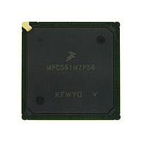
MPC561MZP56 Freescale, MPC561MZP56 Datasheet - Page 741

MPC561MZP56
Manufacturer Part Number
MPC561MZP56
Description
Manufacturer
Freescale
Datasheet
1.MPC561MZP56.pdf
(1420 pages)
Specifications of MPC561MZP56
Cpu Family
MPC56x
Device Core
PowerPC
Device Core Size
32b
Frequency (max)
56MHz
Interface Type
QSPI/SCI/SPI/UART
Total Internal Ram Size
32KB
# I/os (max)
56
Number Of Timers - General Purpose
22
Operating Supply Voltage (typ)
2.6/5V
Operating Supply Voltage (max)
2.7/5.25V
Operating Supply Voltage (min)
2.5/4.75V
On-chip Adc
2(32-chx10-bit)
Instruction Set Architecture
RISC
Operating Temp Range
-40C to 125C
Operating Temperature Classification
Automotive
Mounting
Surface Mount
Pin Count
388
Package Type
BGA
Program Memory Type
ROMLess
Program Memory Size
Not Required
Lead Free Status / RoHS Status
Not Compliant
Available stocks
Company
Part Number
Manufacturer
Quantity
Price
Company:
Part Number:
MPC561MZP56
Manufacturer:
Freescale Semiconductor
Quantity:
10 000
Company:
Part Number:
MPC561MZP56R2
Manufacturer:
Freescale Semiconductor
Quantity:
10 000
- Current page: 741 of 1420
- Download datasheet (11Mb)
17.3.1
The MIOS14 requires 34 signals: 10 MDASM signals, 8 dedicated MPWMSM signals, 12 dedicated
MPIOSM signals and 4 signals are shared between the MPWMSM and MPIOSM. The required signal
function on shared signals is chosen using the PDMCR2 register in the USIU. The usage of all MIOS14
signals is shown in the block diagram of
17.3.2
The internal bus system within the MIOS14 is called the modular I/O bus (MIOB). The MIOB makes
communications possible between any submodule and the IMB3 bus master through the MBISM.
The MIOB is divided into three dedicated buses:
Freescale Semiconductor
MIRSM0
MIRSM1
Reserve
Reserve
MCPSM
Reserve
Reserve
Module
MBISM
Type
Sub-
d
d
d
d
Bloc
259-
384-
392-
400-
No.
255
256
257
258
383
391
399
511
33-
MIOS14 Signals
MIOS14 Bus System
k
BSL0=
BSL1=
CBA
0
0
Table 17-1. MIOS14 Configuration Description (continued)
BSL0=
BSL1=
Connected to:
CBB
1
0
BSL0=0
BSL1=1
CBC
MPC561/MPC563 Reference Manual, Rev. 1.2
BSL0=
BSL1=
CBD
1
1
Figure 17-1
MIRS
No.
M
Position
MIRSM
and in the configuration description of
Bit
Address
Offset
Base
6C00
6C40
0x30
6800
0x30
6810
0x30
0x30
Function
Signal
GPIO
GPIO
GPIO
GPIO
Modular Input/Output Subsystem (MIOS14)
MPIO32
MPIO32
MPIO32
MPIO32
Signal
Name
Input
B12
B13
B14
B15
MPIO32
MPIO32
MPIO32
MPIO32
Output
Signal
Name
B12
B13
B14
B15
Table
C_CNTX0
PPM_TCL
PPM_RX0
PPM_TX0
Alternate
Signal
Name
K
17-1.
17-9
Related parts for MPC561MZP56
Image
Part Number
Description
Manufacturer
Datasheet
Request
R

Part Number:
Description:
MPC5 1K0 5%
Manufacturer:
TE Connectivity
Datasheet:

Part Number:
Description:
MPC5 500R 5%
Manufacturer:
TE Connectivity
Datasheet:

Part Number:
Description:
MPC5 5K0 5%
Manufacturer:
Tyco Electronics
Datasheet:

Part Number:
Description:
MPC5 5R0 5%
Manufacturer:
Tyco Electronics
Datasheet:

Part Number:
Description:
MPC5 50K 5%
Manufacturer:
Tyco Electronics
Datasheet:

Part Number:
Description:
MPC5 1R0 5%
Manufacturer:
Tyco Electronics
Datasheet:

Part Number:
Description:
TOWER ELEVATOR BOARDS HARDWARE
Manufacturer:
Freescale Semiconductor
Datasheet:

Part Number:
Description:
TOWER SERIAL I/O HARDWARE
Manufacturer:
Freescale Semiconductor
Datasheet:

Part Number:
Description:
LCD MODULE FOR TWR SYSTEM
Manufacturer:
Freescale Semiconductor
Datasheet:

Part Number:
Description:
DAUGHTER LCD WVGA I.MX51
Manufacturer:
Freescale Semiconductor
Datasheet:

Part Number:
Description:
TOWER SYSTEM BOARD MPC5125
Manufacturer:
Freescale Semiconductor
Datasheet:


