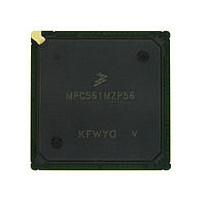
MPC561MZP56 Freescale, MPC561MZP56 Datasheet - Page 443

MPC561MZP56
Manufacturer Part Number
MPC561MZP56
Description
Manufacturer
Freescale
Datasheet
1.MPC561MZP56.pdf
(1420 pages)
Specifications of MPC561MZP56
Cpu Family
MPC56x
Device Core
PowerPC
Device Core Size
32b
Frequency (max)
56MHz
Interface Type
QSPI/SCI/SPI/UART
Total Internal Ram Size
32KB
# I/os (max)
56
Number Of Timers - General Purpose
22
Operating Supply Voltage (typ)
2.6/5V
Operating Supply Voltage (max)
2.7/5.25V
Operating Supply Voltage (min)
2.5/4.75V
On-chip Adc
2(32-chx10-bit)
Instruction Set Architecture
RISC
Operating Temp Range
-40C to 125C
Operating Temperature Classification
Automotive
Mounting
Surface Mount
Pin Count
388
Package Type
BGA
Program Memory Type
ROMLess
Program Memory Size
Not Required
Lead Free Status / RoHS Status
Not Compliant
Available stocks
Company
Part Number
Manufacturer
Quantity
Price
Company:
Part Number:
MPC561MZP56
Manufacturer:
Freescale Semiconductor
Quantity:
10 000
Company:
Part Number:
MPC561MZP56R2
Manufacturer:
Freescale Semiconductor
Quantity:
10 000
- Current page: 443 of 1420
- Download datasheet (11Mb)
Program the region base address in the L2U_RBAx registers to the lower boundary of the region specified
by the corresponding L2U_RAx[RS] field. If the region base address does not correspond to the boundary
of the block size programmed in the L2U_RAx, the DMPU snaps the region base to the lower boundary
of that block. For example, if the block size is programmed to 16 Kbytes for region zero (i.e.,
L2U_RA0[RS] = 0x3) and the region base address is programmed to 0x1FFF(i.e., L2U_RBA0[RBA] =
0x1), then the effective base address of region zero is 0x0. See
External action is required to program only legal region sizes. The L2U does not check whether the value
is legal. If an illegal region size is programmed, the region calculation may not be successful.
11.5.3
All L-bus slaves have their own access protection logic. For consistency, all storage access violations have
the same termination result. Thus access violations for load/store accesses started by the RCPU always
have the same termination from all slaves: assertion of the data storage exception. All other L-bus masters
cause machine check exceptions.
11.6
In general terms, a reservation activity is the process whereby a load and store instruction pair is
accompanied by a reservation of the data, the goal being to achieve an atomic operation. If a bus master
other than the one holding the reservation accesses the data (or some other specific condition occurs as
described in
The RCPU storage reservation protocol supports a multi-level bus structure. For each local bus, storage
reservation is handled by the local reservation logic. The protocol tries to optimize reservation cancellation
such that an MPC500 processor (RCPU) is notified of storage reservation loss on a remote bus (U-bus,
IMB or external bus) only when it has issued a stwcx cycle to that address. That is, the reservation loss
indication comes as part of the stwcx cycle.
Freescale Semiconductor
Reservation Support
L-Bus Memory Access Violations
Section 11.6.1, “Reservation
The appropriate DMPU registers must be programmed before the MSR[DR]
bit is set. Otherwise, DMPU operation is not guaranteed.
0x0000 0000
0x0000 1FFF
0x0000 3FFF
0x0000 5FFF
Figure 11-3. Region Base Address Example
MPC561/MPC563 Reference Manual, Rev. 1.2
(16 Kbytes)
Protocol”) the reservation is lost and is indicated accordingly.
Region 0
NOTE
Figure
Resulting Region
Actual Programmed Region
11-3.
L-Bus to U-Bus Interface (L2U)
11-7
Related parts for MPC561MZP56
Image
Part Number
Description
Manufacturer
Datasheet
Request
R

Part Number:
Description:
MPC5 1K0 5%
Manufacturer:
TE Connectivity
Datasheet:

Part Number:
Description:
MPC5 500R 5%
Manufacturer:
TE Connectivity
Datasheet:

Part Number:
Description:
MPC5 5K0 5%
Manufacturer:
Tyco Electronics
Datasheet:

Part Number:
Description:
MPC5 5R0 5%
Manufacturer:
Tyco Electronics
Datasheet:

Part Number:
Description:
MPC5 50K 5%
Manufacturer:
Tyco Electronics
Datasheet:

Part Number:
Description:
MPC5 1R0 5%
Manufacturer:
Tyco Electronics
Datasheet:

Part Number:
Description:
TOWER ELEVATOR BOARDS HARDWARE
Manufacturer:
Freescale Semiconductor
Datasheet:

Part Number:
Description:
TOWER SERIAL I/O HARDWARE
Manufacturer:
Freescale Semiconductor
Datasheet:

Part Number:
Description:
LCD MODULE FOR TWR SYSTEM
Manufacturer:
Freescale Semiconductor
Datasheet:

Part Number:
Description:
DAUGHTER LCD WVGA I.MX51
Manufacturer:
Freescale Semiconductor
Datasheet:

Part Number:
Description:
TOWER SYSTEM BOARD MPC5125
Manufacturer:
Freescale Semiconductor
Datasheet:


