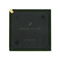
MPC561MZP56 Freescale, MPC561MZP56 Datasheet - Page 945

MPC561MZP56
Manufacturer Part Number
MPC561MZP56
Description
Manufacturer
Freescale
Datasheet
1.MPC561MZP56.pdf
(1420 pages)
Specifications of MPC561MZP56
Cpu Family
MPC56x
Device Core
PowerPC
Device Core Size
32b
Frequency (max)
56MHz
Interface Type
QSPI/SCI/SPI/UART
Total Internal Ram Size
32KB
# I/os (max)
56
Number Of Timers - General Purpose
22
Operating Supply Voltage (typ)
2.6/5V
Operating Supply Voltage (max)
2.7/5.25V
Operating Supply Voltage (min)
2.5/4.75V
On-chip Adc
2(32-chx10-bit)
Instruction Set Architecture
RISC
Operating Temp Range
-40C to 125C
Operating Temperature Classification
Automotive
Mounting
Surface Mount
Pin Count
388
Package Type
BGA
Program Memory Type
ROMLess
Program Memory Size
Not Required
Lead Free Status / RoHS Status
Not Compliant
Available stocks
Company
Part Number
Manufacturer
Quantity
Price
Company:
Part Number:
MPC561MZP56
Manufacturer:
Freescale Semiconductor
Quantity:
10 000
Company:
Part Number:
MPC561MZP56R2
Manufacturer:
Freescale Semiconductor
Quantity:
10 000
- Current page: 945 of 1420
- Download datasheet (11Mb)
The trap enable control register is not accessed by the CPU, but instead supplies signals to the CPU. The
trap enable bits, VSYNC bit, and the breakpoint bits of this register are loaded from the development port
shift register as the result of trap enable mode transmissions. The trap enable bits are reflected in ICTRL
and LCTRL2 special registers. See
Section 23.6.10, “L-Bus Support Control Register
23.4.6.3
The development port shift register is selected when the CPU accesses DPIR or DPDR. Accesses to these
two special purpose registers occur in debug mode and appear on the internal bus as an address and the
assertion of an address attribute signal indicating that a special purpose register is being accessed. The
DPIR register is read by the CPU to fetch all instructions when in debug mode and the DPDR register is
read and written to transfer data between the CPU and external development tools. The DPIR and DPDR
are pseudo registers. Decoding either of these registers will cause the development port shift register to be
accessed. The debug mode logic knows whether the CPU is fetching instructions or reading or writing
data. If what the CPU is expecting and what the register receives from the serial port do not match
(instruction instead of data) the mismatch is used to signal a sequence error to the external development
tool.
23.4.6.4
All of the serial transmissions are clock transmissions and are therefore synchronous communications.
However, the transmission clock may be either synchronous or asynchronous with the system clock
(CLKOUT). The development port allows the selection of two methods for clocking the serial
transmissions. The first method allows the transmission to occur without being externally synchronized
with CLKOUT, in this mode a serial clock DSCK must be supplied to the MPC561/MPC563. The other
communication method requires a data to be externally synchronized with CLKOUT.
The first clock mode is called “asynchronous clock” since the input clock (DSCK) is asynchronous with
CLKOUT. To be sure that data on DSDI is sampled correctly, transitions on DSDI must occur a setup time
ahead and a hold time after the rising edge of DSCK. This clock mode allows communications with the
port from a development tool which does not have access to the CLKOUT signal or where the CLKOUT
signal has been delayed or skewed. Refer to the timing diagram in
The second clock mode is called “synchronous self clock”. It does not require an input clock. Instead the
port is timed by the system clock. The DSDI input is required to meet setup and hold time requirements
with respect to CLKOUT rising edge. The data rate for this mode is always the same as the system clock.
Refer to the timing diagram in
The selection of clock or self clock mode is made at reset. The state of the DSDI input is latched eight
clocks after SRESET negates. If it is latched low, asynchronous clock mode is enabled. If it is latched high
then synchronous self clock mode is enabled.
Since DSDI is used to select the development port clocking scheme, it is necessary to prevent any
transitions on DSDI during this time from being recognized as the start of a serial transmission. The port
will not begin scanning for the start bit of a serial transmission until 16 clocks after the negation of
SRESET. If DSDI is asserted 16 clocks after SRESET negation, the port will wait until DSDI is negated
to begin scanning for the start bit.
Freescale Semiconductor
Development Port Registers Decode
Development Port Serial Communications — Clock Mode Selection
Figure
MPC561/MPC563 Reference Manual, Rev. 1.2
Section 23.6.10, “L-Bus Support Control Register
23-10.
2.”
Figure
23-9.
2” and
Development Support
23-31
Related parts for MPC561MZP56
Image
Part Number
Description
Manufacturer
Datasheet
Request
R

Part Number:
Description:
MPC5 1K0 5%
Manufacturer:
TE Connectivity
Datasheet:

Part Number:
Description:
MPC5 500R 5%
Manufacturer:
TE Connectivity
Datasheet:

Part Number:
Description:
MPC5 5K0 5%
Manufacturer:
Tyco Electronics
Datasheet:

Part Number:
Description:
MPC5 5R0 5%
Manufacturer:
Tyco Electronics
Datasheet:

Part Number:
Description:
MPC5 50K 5%
Manufacturer:
Tyco Electronics
Datasheet:

Part Number:
Description:
MPC5 1R0 5%
Manufacturer:
Tyco Electronics
Datasheet:

Part Number:
Description:
TOWER ELEVATOR BOARDS HARDWARE
Manufacturer:
Freescale Semiconductor
Datasheet:

Part Number:
Description:
TOWER SERIAL I/O HARDWARE
Manufacturer:
Freescale Semiconductor
Datasheet:

Part Number:
Description:
LCD MODULE FOR TWR SYSTEM
Manufacturer:
Freescale Semiconductor
Datasheet:

Part Number:
Description:
DAUGHTER LCD WVGA I.MX51
Manufacturer:
Freescale Semiconductor
Datasheet:

Part Number:
Description:
TOWER SYSTEM BOARD MPC5125
Manufacturer:
Freescale Semiconductor
Datasheet:


